© Semiconductor Components Industries, LLC, 2005
November, 2005 − Rev. 2
1 Publication Order Number:
NB2308A/D
NB2308A
3.3 V Zero Delay
Clock Buffer
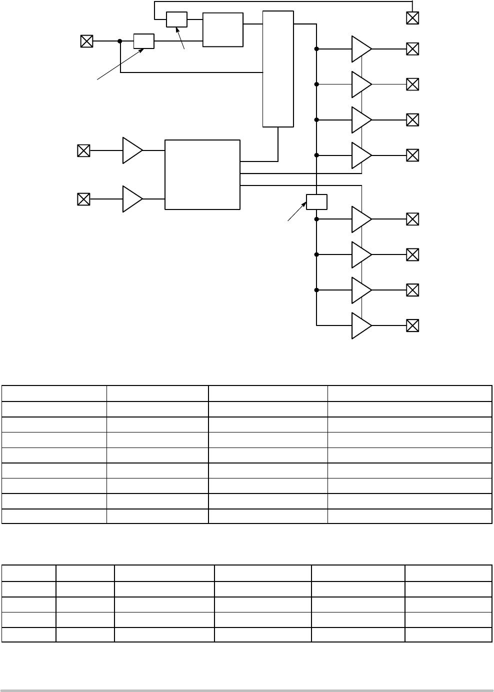
The NB2308A is a versatile, 3.3 V zero delay buffer designed to
distribute high−speed clocks. It is available in a 16 pin package. The
part has an on−chip PLL which locks to an input clock presented on
the REF pin. The PLL feedback is required to be driven to FBK pin,
and can be obtained from one of the outputs. The input−to−output
propagation delay is guaranteed to be less than 250 ps, and the
output−to−output skew is guaranteed to be less than 200 ps.
The NB2308A has two banks of four outputs each, which can be
controlled by the select inputs as shown in the Select Input Decoding
Table. If all the output clocks are not required, Bank B can be
three−stated. The select input also allows the input clock to be directly
applied to the outputs for chip and system testing purposes.
Multiple NB2308A devices can accept the same input clock and
distribute it. In this case the skew between the outputs of the two
devices is guaranteed to be less than 700 ps.
The NB2308A is available in five different configurations (Refer to
NB2308A Configurations Table). The NB2308Ax1* is the base part,
where the output frequencies equal the reference if there is no counter
in the feedback path. The NB2308Ax1H is the high−drive version of
the −1 and the rise and fall times on this device are much faster.
The NB2308Ax2 allows the user to obtain 2X and 1X frequencies
on each output bank. The exact configuration and output frequencies
depends on which output drives the feedback pin. The NB2308Ax3
allows the user to obtain 4X and 2X frequencies on the outputs.
The NB2308Ax4 enables the user to obtain 2X clocks on all outputs.
Thus, the part is extremely versatile, and can be used in a variety of
applications.
The NB2308Ax5H is a high−drive version with REF/2 on both
banks.
Features
• Zero Input − Output Propagation Delay, Adjustable by Capacitive
Load on FBK Input
• Multiple Configurations − Refer to NB2308A Configurations Table
• Input Frequency Range: 15 MHz to 133 MHz
• Multiple Low−Skew Outputs
• Output−Output Skew Less than 200 ps
• Device−Device Skew Less than 700 ps
• Two banks of four outputs, three−stateable by two select inputs
• Less than 200 ps Cycle−to−Cycle Jitter
• Available in 16−pin SOIC and TSSOP Packages
• 3.3V operation
• Advanced 0.35 CMOS Technology
• Pb−Free Packages are Available**
*x = C for Commercial; I for Industrial.
**For additional information on our Pb−Free strategy and soldering details,
please download the ON Semiconductor Soldering and Mounting Techniques
Reference Manual, SOLDERRM/D.
MARKING
DIAGRAMS*
XXXX = Device Code
A = Assembly Location
WL, L = Wafer Lot
Y = Year
WW, W = Work Week
G or G = Pb−Free Package
(Note: Microdot may be in either location)
*For additional marking information, refer to
Application Note AND8002/D.
See detailed ordering and shipping information in the package
dimensions section on page 9 of this data sheet.
ORDERING INFORMATION
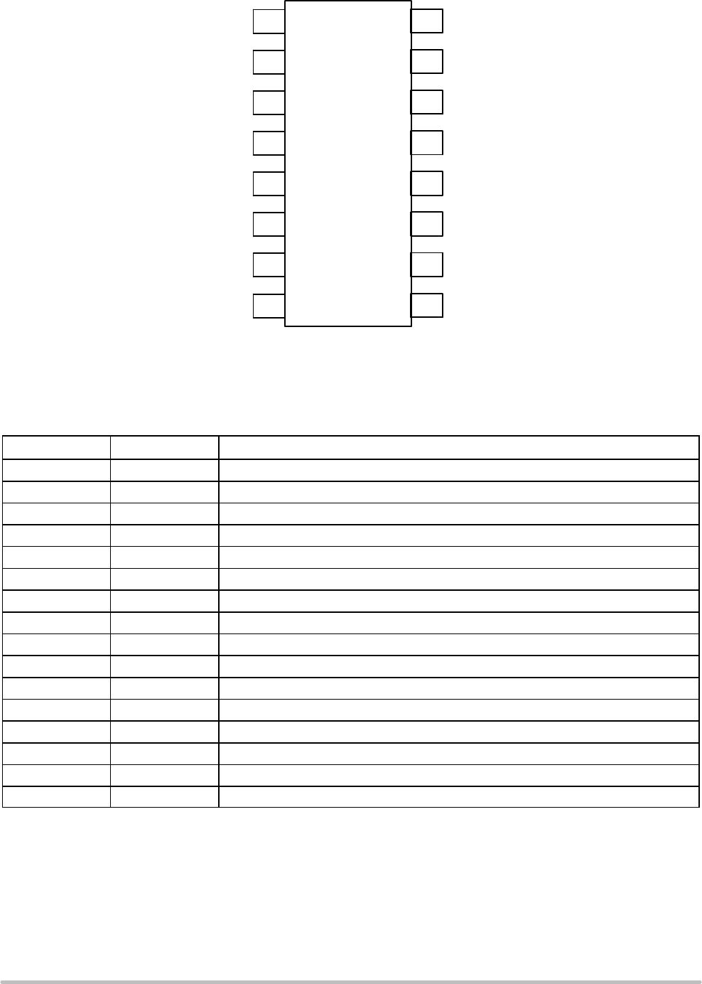
http://onsemi.com
SOIC−16
D SUFFIX
CASE 751B
1
16
1
16
1
16
1
16
XXXX
XXXX
ALYWG
G
XXXXXXXXXG
AWLYWW
TSSOP−16
DT SUFFIX
CASE 948F