4
Rev. 1.8
08/20/02
IRU1050
www.irf.com
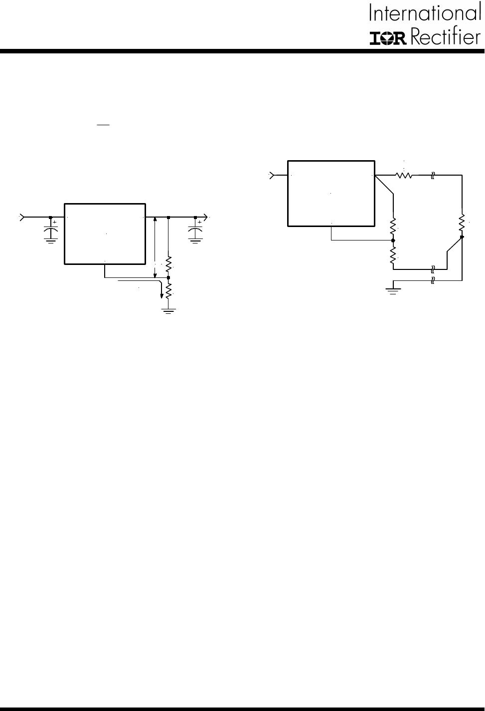
Output Voltage Setting
The IRU1050 can be programmed to any voltages in the
range of 1.25V to 5.5V with the addition of R1 and R2
external resistors according to the following formula:
Where:
VREF = 1.25V Typically
IADJ = 50mA Typically
R1 and R2 as shown in Figure 3:
Figure 3 - Typical application of the IRU1050
for programming the output voltage.
The IRU1050 keeps a constant 1.25V between the out-
put pin and the adjust pin. By placing a resistor R1 across
these two pins a constant current flows through R1, add-
ing to the IADJ current and into the R2 resistor producing
a voltage equal to the (1.25/R1)3R2 + IADJ3R2 which
will be added to the 1.25V to set the output voltage.
This is summarized in the above equation. Since the
minimum load current requirement of the IRU1050 is
10mA, R1 is typically selected to be 121V resistor so
that it automatically satisfies the minimum current re-
quirement. Notice that since IADJ is typically in the range
of 50mA it only adds a small error to the output voltage
and should only be considered when a very precise out-
put voltage setting is required. For example, in a typical
3.3V application where R1=121V and R2=200V the er-
ror due to IADJ is only 0.3% of the nominal set point.
Load Regulation
Since the IRU1050 is only a three-terminal device, it is
not possible to provide true remote sensing of the output
voltage at the load. Figure 4 shows that the best load
regulation is achieved when the bottom side of R2 is
connected to the load and the top side of R1 resistor is
connected directly to the case or the VOUT pin of the
regulator and not to the load. In fact, if R1 is connected
to the load side, the effective resistance between the
regulator and the load is gained up by the factor of (1+R2/
R1), or the effective resistance will be RP(eff)=RP3(1+R2/
R1). It is important to note that for high current applica-
tions, this can represent a significant percentage of the
overall load regulation and one must keep the path from
the regulator to the load as short as possible to mini-
mize this effect.
Figure 4 - Schematic showing connection
for best load regulation.
Stability
The IRU1050 requires the use of an output capacitor as
part of the frequency compensation in order to make the
regulator stable. Typical designs for microprocessor ap-
plications use standard electrolytic capacitors with a
typical ESR in the range of 50 to 100mV and an output
capacitance of 500 to 1000mF. Fortunately as the ca-
pacitance increases, the ESR decreases resulting in a
fixed RC time constant. The IRU1050 takes advantage
of this phenomena in making the overall regulator loop
stable. For most applications a minimum of 100mF alu-
minum electrolytic capacitor such as Sanyo MVGX se-
ries, Panasonic FA series as well as the Nichicon PL
series insures both stability and good transient response.
Thermal Design
The IRU1050 incorporates an internal thermal shutdown
that protects the device when the junction temperature
exceeds the maximum allowable junction temperature.
Although this device can operate with junction tempera-
tures in the range of 1508C, it is recommended that the
selected heat sink be chosen such that during maxi-
mum continuous load operation the junction tempera-
ture is kept below this number. The example below shows
the steps in selecting the proper regulator heat sink for
the worst case current consumption using Intel 200MHz
microprocessor as the load.
VOUT
R1
R2
VIN
VREF
IADJ = 50uA
Adj
VOUT
VIN
IRU1050
R1
R2
V
IN
R
L
R
P
PARASITIC LINE
RESISTANCE
IRU1050
Adj
V
OUT
Vin
VOUT = VREF3 1+ +IADJ3R2
R2
R1
( )
IRU1050
5
Rev. 1.8
08/20/02
www.irf.com
Assuming the following specifications:
The steps for selecting a proper heat sink to keep the
junction temperature below 1358C is given as:
1) Calculate the maximum power dissipation using:
2) Select a package from the regulator data sheet and
record its junction to case (or tab) thermal resistance.
Selecting TO-220 package gives us:
3) Assuming that the heat sink is black anodized, cal-
culate the maximum heat sink temperature allowed:
Assume, ucs=0.05°C/W (heat-sink-to-case thermal
resistance for black anodized)
4) With the maximum heat sink temperature calculated
in the previous step, the heat-sink-to-air thermal re-
sistance (uSA) is calculated by first calculating the
temperature rise above the ambient as follows:
5) Next, a heat sink with lower uSA than the one calcu-
lated in Step 4 must be selected. One way to do this
is to simply look at the graphs of the “Heat Sink Temp
Rise Above the Ambient” vs. the “Power Dissipation”
and select a heat sink that results in lower tempera-
ture rise than the one calculated in previous step.
The following heat sinks from AAVID and Thermalloy
meet this criteria.
PD = IOUT3(VIN - VOUT)
PD = 4.63(5 - 3.5) = 6.9W
VIN = 5V
VOUT = 3.5V
IOUT(MAX) = 4.6A
TA = 358C
uJC = 2.78C/W
TS = TJ - PD3(uJC + uCS)
TS = 135 - 6.93(27 + 0.05) = 1168C
uSA = = = 11.78C/W
DT
PD
81
6.9
DT = TS - TA = 116 - 35 = 818C
T = Temperature Rise Above Ambient
Note: For further information regarding the above com-
panies and their latest product offerings and application
support contact your local representative or the num-
bers listed below:
AAVID.................PH# (603) 528 3400
Thermalloy...........PH# (214) 243-4321
Designing for Microprocessor Applications
As it was mentioned before, the IRU1050 is designed
specifically to provide power for the new generation of
the low voltage processors requiring voltages in the range
of 2.5V to 3.6V generated by stepping down the 5V sup-
ply. These processors demand a fast regulator that sup-
ports their large load current changes. The worst case
current step seen by the regulator is anywhere in the
range of 1 to 7A with the slew rate of 300 to 500ns which
could happen when the processor transitions from “Stop
Clock” mode to the “Full Active” mode. The load current
step at the processor is actually much faster, in the or-
der of 15 to 20ns, however, the decoupling capacitors
placed in the cavity of the processor socket handle this
transition until the regulator responds to the load current
levels. Because of this requirement the selection of high
frequency low ESR and low ESL output capacitor is
imperative in the design of these regulator circuits.
Figure 5 shows the effects of a fast transient on the
output voltage of the regulator. As shown in this figure,
the ESR of the output capacitor produces an instanta-
neous drop equal to the (DVESR=ESR3DI) and the ESL
effect will be equal to the rate of change of the output
current times the inductance of the capacitor. (DVESL
=L3DI/Dt). The output capacitance effect is a droop in
the output voltage proportional to the time it takes for
the regulator to respond to the change in the current,
(DVc=Dt3DI/C) where Dt is the response time of the
regulator.
Air Flow (LFM)
0 100 200 300 400
Thermalloy 6021PB 6021PB 6073PB 6109PB 7141D
AAVID 534202B 534202B 507302 575002 576802B
6
Rev. 1.8
08/20/02
IRU1050
www.irf.com
V
ESR
V
ESL
V
C
T
LOAD
CURRENT
LOAD CURRENT RISE TIME
1050plt1-1.0
DVc = = = 1.2mV
Dt 3 DI 2 3 4.6
C 7500
CIN = = 1530mF
4.6 3 50
0.15
ESR =
(VIN - VOUT - DV - VDROP)
DI
ESR = = 0.032V
(5 - 3.5 - 1.2 - 0.15)
4.6
ESR [ = 8mV
37
4.6
Type of VOUT IMAX Max Allowed
Processor Nominal Output Tolerance
Intel-P54C VRE 3.50 V 4.6 A ±100 mV
Figure 5 - Typical regulator response
to the fast load current step.
An example of a regulator design to meet the Intel P54C
VRE specification is given below.
Assume the specification for the processor as shown in
Table 1:
Table 1 - Processor Specification
The first step is to select the voltage step allowed in the
output due to the output capacitor’s ESR:
1) Assuming the regulator’s initial accuracy plus the re-
sistor divider tolerance is ≈ ±53mV (±1.5% of 3.5V
nominal), then the total step allowed for the ESR and
the ESL is 47mV.
Assuming that the ESL drop is 10mV, the remain-
ing ESR step will be37mV. Therefore the output
capacitor ESR must be:
The Sanyo MVGX series is a good choice to achieve
both price and performance goals. The 6MV1500GX,
1500mF, 6.3V has an ESR of less than 36mV typi-
cal. Selecting 5 of these capacitors in parallel has an
ESR of 7.2mV which achieves our design goal.
The next step is to calculate the drop due to the ca-
pacitance discharge and make sure that this drop in
voltage is less than the selected ESL drop in the
previous step.
R2 = 3R1 = 3121 = 217.8V
VOUT
VREF
-1
( )
3.5
1.25
-1
( )
2) The output capacitance is 531500mF = 7500mF
Where:
Dt = 2ms is the regulator response time
To set the output DC voltage, we need to select R1 and
R2:
3) Assuming R1=121V, 0.1%:
Select R2=218V, 0.1%
Selecting both R1 and R2 resistors to be 0.1% toler-
ance, results in the least amount of error introduced
by the resistor dividers leaving ≈ ±1.3% error budget
for the IRU1050 reference which is within the initial
accuracy of the device.
Finally, the input capacitor is selected as follows:
4) Assuming that the input voltage can drop 150mV be-
fore the main power supply responds, and that the
main power supply response time is 50ms, then
the minimum input capacitance for a 4.6A load step
is given by:
The ESR should be less than:
Where:
VDROP L Input voltage drop allowed in step 4
DV L Maximum regulator dropout voltage
DI L Load current step
Selecting two Sanyo 1500mF, the same type as the
output capacitors, meets our requirements.

IRU1050CP

Mfr. #:
Manufacturer:
Infineon Technologies
Description:
IC REG LIN POS ADJ 5A 2-UTHINPAK
Lifecycle:
New from this manufacturer.
Delivery:
DHL FedEx Ups TNT EMS
Payment:
T/T Paypal Visa MoneyGram Western Union