IRU1050
7
Rev. 1.8
08/20/02
www.irf.com
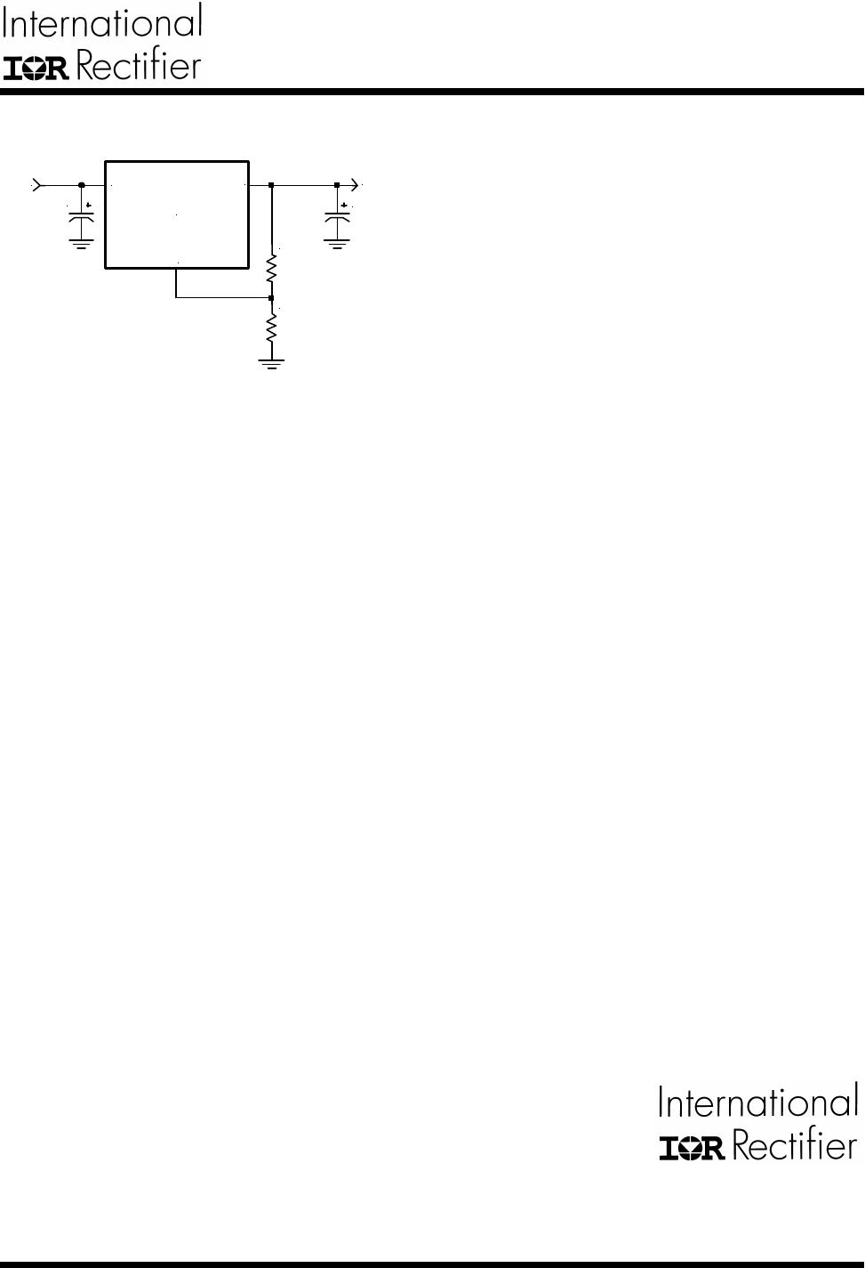
Layout Consideration
The output capacitors must be located as close to the
VOUT terminal of the device as possible. It is recom-
mended to use a section of a layer of the PC board as a
plane to connect the VOUT pin to the output capacitors to
prevent any high frequency oscillation that may result
due to excessive trace inductance.
Figure 6 shows the completed schematic for our ex-
ample.
Figure 6 - Final schematic for
the Intel VRE application.
IR WORLD HEADQUARTERS: 233 Kansas St., El Segundo, California 90245, USA Tel: (310) 252-7105
TAC Fax: (310) 252-7903
Visit us at www.irf.com for sales contact information
Data and specifications subject to change without notice. 02/01
3.50V
R1
121
0.1%
R2
218
0.1%
5V
C2
5x 1500uF
C1
1500uF
IRU1050
Adj
VOUT
VIN