MP28265 – 5A, 21V, SYNCHRONOUS STEP-DOWN CONVERTER WITH INTERNAL MOSFETS
MP28265 Rev. 0.92 www.MonolithicPower.com 10
12/2/2009 MPS Proprietary Information. Unauthorized Photocopy and Duplication Prohibited.
© 2009 MPS. All Rights Reserved.
Vin
EN/Sync
Vcc
Vout
CLK
5us
Foldback
1.1MHz
External CLK
0.625*Vout_set
2ms1ms
V
CC_Rising
Vout_set
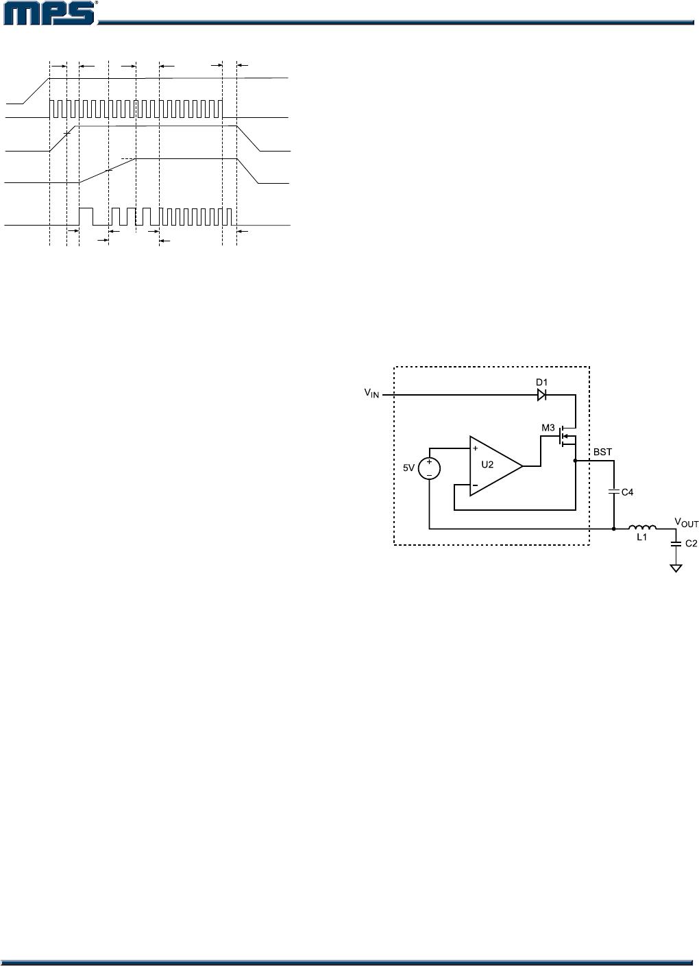
Figure 4—Startup Sequence Using External
Sync Clock Signal
Under-Voltage Lockout (UVLO)
Under-voltage lockout (UVLO) is implemented to
protect the chip from operating at insufficient
supply voltage. The MP28265 UVLO comparator
monitors the output voltage of the internal
regulator, VCC. The UVLO rising threshold is
about 4.0V while its falling threshold is a
consistent 3.2V.
Internal Soft-Start
The soft-start is implemented to prevent the
converter output voltage from overshooting
during startup. When the chip starts, the internal
circuitry generates a soft-start voltage (SS)
ramping up from 0V to 1.2V. When it is lower
than the internal reference (REF), SS overrides
REF so the error amplifier uses SS as the
reference. When SS is higher than REF, REF
regains control. The SS time is internally fixed to
4ms.
Over-Current-Protection and Hiccup
The MP28265 has cycle-by-cycle over current
limit when the inductor current peak value
exceeds the set current limit threshold.
Meanwhile, output voltage starts to drop until FB
is below the Under-Voltage (UV) threshold,
typically 30% below the reference. Once a UV is
triggered, the MP28265 enters hiccup mode to
periodically restart the part. This protection mode
is especially useful when the output is dead-short
to ground. The average short circuit current is
greatly reduced to alleviate the thermal issue and
to protect the regulator. The MP28265 exits the
hiccup mode once the over current condition is
removed.
Thermal Shutdown
Thermal shutdown is implemented to prevent the
chip from operating at exceedingly high
temperatures. When the silicon die temperature
is higher than 150°C, it shuts down the whole
chip. When the temperature is lower than its
lower threshold, typically 140°C, the chip is
enabled again.
Floating Driver and Bootstrap Charging
The floating power MOSFET driver is powered by
an external bootstrap capacitor. This floating
driver has its own UVLO protection. This UVLO’s
rising threshold is 2.2V with a hysteresis of
150mV. The bootstrap capacitor voltage is
regulated internally by VIN through D1, M3, C4,
L1 and C2 (Figure 5). If (VIN-VSW) is more than
5V, U2 will regulate M3 to maintain a 5V BST
voltage across C4.
SW
Figure 5—Internal Bootstrap Charging Circuit
Startup and Shutdown
If both VIN and EN are higher than their
appropriate thresholds, the chip starts. The
reference block starts first, generating stable
reference voltage and currents, and then the
internal regulator is enabled. The regulator
provides stable supply for the remaining
circuitries.
Three events can shut down the chip: EN low,
VIN low and thermal shutdown. In the shutdown
procedure, the signaling path is first blocked to
avoid any fault triggering. The COMP voltage and
the internal supply rail are then pulled down. The
floating driver is not subject to this shutdown
command
.
MP28265 – 5A, 21V, SYNCHRONOUS STEP-DOWN CONVERTER WITH INTERNAL MOSFETS
MP28265 Rev. 0.92 www.MonolithicPower.com 11
12/2/2009 MPS Proprietary Information. Unauthorized Photocopy and Duplication Prohibited.
© 2009 MPS. All Rights Reserved.
APPLICATION INFORMATION
Setting the Output Voltage
The external resistor divider is used to set the
output voltage (see Typical Application on page
1). The feedback resistor R1 also sets the
feedback loop bandwidth with the internal
compensation capacitor (see Typical Application
on page 1). Choose R1 to be around 40.2k for
optimal transient response. R2 is then given by:
1
V
V
R1
R2
FB
OUT
=
The T-type network is highly recommended when
Vo is low, as Figure 6 shows.
FB
1
R2
R1
Rt
VOUT
Figure 6— T-type Network
Table 1 lists the recommended T-type resistors
value for common output voltages.
Table 1—Resistor Selection for Common
Output Voltages
V
OUT
(V) R1 (k) R2 (k) Rt (k)
1.05 4.99(1%) 16.5(1%) 24.9(1%)
1.2 4.99(1%) 10.2(1%) 24.9(1%)
1.5 4.99(1%) 5.76(1%) 24.9(1%)
1.8 4.99(1%) 4.02(1%) 24.9(1%)
2.5 40.2 (1%) 19.1(1%) 0
3.3 40.2(1%) 13(1%) 0
5 40.2 (1%) 7.68(1%) 0
Selecting the Inductor
A 1µH to 10µH inductor with a DC current rating
of at least 25% percent higher than the maximum
load current is recommended for most
applications. For highest efficiency, the inductor
DC resistance should be less than 15m. For
most designs, the inductance value can be
derived from the following equation.
OSCLIN
OUTINOUT
fIV
)VV(V
L
×Δ×
×
=
Where I
L
is the inductor ripple current.
Choose inductor ripple current to be
approximately 30% if the maximum load current,
5A. The maximum inductor peak current is:
2
I
II
L
LOAD)MAX(L
Δ
+=
Under light load conditions below 100mA, larger
inductance is recommended for improved
efficiency.
Selecting the Input Capacitor
The input current to the step-down converter is
discontinuous, therefore a capacitor is required to
supply the AC current to the step-down converter
while maintaining the DC input voltage. Use low ESR
capacitors for the best performance. Ceramic
capacitors with X5R or X7R dielectrics are highly
recommended because of their low ESR and
small temperature coefficients. For most
applications, a 22µF capacitor is sufficient.
Since the input capacitor (C1) absorbs the input
switching current it requires an adequate ripple
current rating. The RMS current in the input capacitor
can be estimated by:
×
×=
IN
OUT
IN
OUT
LOAD1C
V
V
1
V
V
II
The worse case condition occurs at V
IN = 2VOUT,
where:
2
I
I
LOAD
1C
=
For simplification, choose the input capacitor
whose RMS current rating greater than half of the
maximum load current.
The input capacitor can be electrolytic, tantalum
or ceramic. When using electrolytic or tantalum
capacitors, a small, high quality ceramic
capacitor, i.e. 0.1F, should be placed as close
to the IC as possible. When using ceramic
capacitors, make sure that they have enough
capacitance to provide sufficient charge to
prevent excessive voltage ripple at input. The
input voltage ripple caused by capacitance can
be estimated by:
××
×
=Δ
IN
OUT
IN
OUT
S
LOAD
IN
V
V
1
V
V
1Cf
I
V
MP28265 – 5A, 21V, SYNCHRONOUS STEP-DOWN CONVERTER WITH INTERNAL MOSFETS
MP28265 Rev. 0.92 www.MonolithicPower.com 12
12/2/2009 MPS Proprietary Information. Unauthorized Photocopy and Duplication Prohibited.
© 2009 MPS. All Rights Reserved.
Selecting the Output Capacitor
The output capacitor (C2) is required to
maintain the DC output voltage. Ceramic,
tantalum, or low ESR electrolytic capacitors are
recommended. Low ESR capacitors are
preferred to keep the output voltage ripple low.
The output voltage ripple can be estimated by:
××
+×
×
×
=Δ
2Cf8
1
R
V
V
1
Lf
V
V
S
ESR
IN
OUT
S
OUT
OUT
Where L is the inductor value and R
ESR is the
equivalent series resistance (ESR) value of the
output capacitor.
In the case of ceramic capacitors, the
impedance at the switching frequency is
dominated by the capacitance. The output
voltage ripple is mainly caused by the
capacitance. For simplification, the output
voltage ripple can be estimated by:
×
×××
=
IN
OUT
2
S
OUT
OUT
V
V
1
2CLf8
V
V
In the case of tantalum or electrolytic capacitors,
the ESR dominates the impedance at the
switching frequency. For simplification, the
output ripple can be approximated to:
ESR
IN
OUT
S
OUT
OUT
R
V
V
1
Lf
V
V ×
×
×
=
The characteristics of the output capacitor also
affect the stability of the regulation system. The
MP28265 can be optimized for a wide range of
capacitance and ESR values.
PCB Layout
PCB layout is very important to achieve stable
operation. Please follow these guidelines and
take Figure 7 for references.
1) Keep the connection of input ground and
GND pin as short and wide as possible.
2) Keep the connection of input capacitor and
IN pin as short and wide as possible.
3) Ensure all feedback connections are short
and direct. Place the feedback resistors
and compensation components as close to
the chip as possible.
4) Route SW away from sensitive analog
areas such as FB.
5) Connect IN, SW, and especially GND
respectively to a large copper area to cool
the chip to improve thermal performance
and long-term reliability.
6) Adding RC snubber circuit from IN pin to
SW pin can reduce SW spikes.
C4
Top Layer
Bottom Layer
Figure 7—PCB Layout

MP28265EL-LF-P

Mfr. #:
Manufacturer:
Monolithic Power Systems (MPS)
Description:
Switching Voltage Regulators 5A, 21V, 1.1MHz Sync Step-down Converter
Lifecycle:
New from this manufacturer.
Delivery:
DHL FedEx Ups TNT EMS
Payment:
T/T Paypal Visa MoneyGram Western Union

Products related to this Datasheet