AD8629TRZ-EP

Zero-Drift, Single-Supply, Rail-to-Rail
Input/Output Operational Amplifier
Data Sheet
AD8629-EP
Rev. A Document Feedback
Information furnished by Analog Devices is believed to be accurate and reliable. However, no
responsibility is assumed by Analog Devices for its use, nor for any infringements of patents or other
rights of third parties that may result from its use. Specifications subject to change without notice. No
license is granted by implication or otherwise under any patent or patent rights of Analog Devices.
Trademarks and registered trademarks are the property of their respective owners.
One Technology Way, P.O. Box 9106, Norwood, MA 02062-9106, U.S.A.
Tel: 781.329.4700 ©2002–2015 Analog Devices, Inc. All rights reserved.
Technical Support www.analog.com
FEATURES
Lowest auto-zero amplifier noise
Low offset voltage: 1 μV typical
Input offset drift: 0.002 μV/°C typical
Rail-to-rail input and output swing
5 V single-supply operation
High gain, CMRR, and PSRR: 130 dB
Very low input bias current: 100 pA maximum
Low supply current: 1.0 mA
Overload recovery time: 50 μs
No external components required
ENHANCED PRODUCT FEATURES
Supports defense and aerospace applications (AQEC standard)
Extended temperature range: −55°C to +125°C
Controlled manufacturing baseline
One assembly/test site
One fabrication site
Enhanced product change notification
Qualification data available on request
APPLICATIONS
Pressure and position sensors
Strain gage amplifiers
Medical instrumentation
Thermocouple amplifiers
Precision current sensing
Photodiode amplifiers
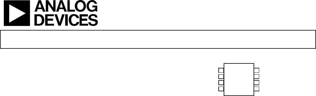
PIN CONFIGURATION
OUT A
1
–IN A
2
+IN A
3
V–
4
V+
8
OUT B
7
–IN B
6
+IN B
5
AD8629-EP
TOP VIEW
(Not to Scale)
12890-001
Figure 1. 8-Lead SOIC_N (R-8)
GENERAL DESCRIPTION
The AD8629-EP amplifier has ultralow offset, drift, and bias
current. The device is a wide bandwidth auto-zero amplifier
featuring rail-to-rail input and output swing and low noise.
Operation is fully specified from 2.7 V to 5 V single supply
(±1.35 V to ±2.5 V dual supply).
The AD8629-EP provides benefits previously found only in
expensive auto-zeroing or chopper-stabilized amplifiers. Using
Analog Devices, Inc., topology, this zero-drift amplifier
combines low cost with high accuracy and low noise. No
external capacitor is required. In addition, the AD8629-EP
greatly reduces the digital switching noise found in most
chopper-stabilized amplifiers.
With an offset voltage of only 1 µV, drift of less than 0.05 V/°C,
and noise of only 0.5 µV p-p (0 Hz to 10 Hz), the AD8629-EP is
suited for applications where error sources cannot be tolerated.
Position and pressure sensors, medical equipment, and strain
gage amplifiers benefit greatly from nearly zero drift over the
operating temperature range. Many systems can take advantage
of the rail-to-rail input and output swings provided by the
AD8629-EP to reduce input biasing complexity and maximize
SNR.
The AD8629-EP is specified for the extended industrial
temperature range (−55°C to +125°C). The AD8629-EP is
available in a standard 8-lead narrow SOIC plastic package.
AD8629-EP Data Sheet
Rev. A | Page 2 of 8
TABLE OF CONTENTS
Features .............................................................................................. 1
Enhanced Product Features ............................................................ 1
Applications ....................................................................................... 1
Pin Configuration ............................................................................. 1
General Description ......................................................................... 1
Revision History ............................................................................... 2
Specifications ..................................................................................... 3
Electrical Characteristics—V
S
= 5.0 V ....................................... 3
Electrical Characteristics—V
S
= 2.7 V........................................4
Absolute Maximum Ratings ............................................................5
Thermal Characteristics ...............................................................5
ESD Caution...................................................................................5
Typical Performance Characteristics ..............................................6
Outline Dimensions ..........................................................................8
Ordering Guide .............................................................................8
REVISION HISTORY
8/15Rev. 0 to Rev. A
Changes to Ordering Guide ............................................................ 8
6/15Revision 0: Initial Version
Data Sheet AD8629-EP
Rev. A | Page 3 of 8
SPECIFICATIONS
ELECTRICAL CHARACTERISTICS—V
S
= 5.0 V
V
S
= 5.0 V, V
CM
= 2.5 V, T
A
= 25°C, unless otherwise noted.
Table 1.
Parameter Symbol Test Conditions/Comments Min Typ Max Unit
INPUT CHARACTERISTICS
Offset Voltage V
OS
1 5 µV
55°C T
A
+125°C
15 µV
Input Bias Current I
B
30 100 pA
55°C T
A
+125°C
1.5 nA
Input Offset Current I
OS
50 200 pA
55°C T
A
+125°C
250 pA
Input Voltage Range
0
5 V
Common-Mode Rejection Ratio CMRR V
CM
= 0 V to 5 V 120 140
dB
55°C T
A
+125°C 115 130
dB
Large Signal Voltage Gain A
VO
R
L
= 10 k, V
O
= 0.3 V to 4.7 V 125 145
dB
55°C T
A
+125°C 120 135
dB
Offset Voltage Drift ∆V
OS
/∆T 55°C T
A
+125°C
0.008 0.05 µV/°C
OUTPUT CHARACTERISTICS
Output Voltage High V
OH
R
L
= 100 kto ground 4.99 4.996
V
55°C T
A
+125°C 4.99 4.995
V
R
L
= 10 kto ground 4.95 4.98
V
55°C T
A
+125°C 4.95 4.97
V
Output Voltage Low V
OL
R
L
= 100 kto V+
1 5 mV
55°C T
A
+125°C
2 5 mV
R
L
= 10 kto V+
10 20 mV
55°C T
A
+125°C
15 20 mV
Short-Circuit Limit I
SC
±25 ±50
mA
55°C T
A
+125°C
±40
mA
Output Current I
O
±30
mA
55°C T
A
+125°C
±15
mA
POWER SUPPLY
Power Supply Rejection Ratio PSRR V
S
= 2.7 V to 5.5 V, 55°C T
A
+125°C 115 130
dB
Supply Current per Amplifier I
SY
V
O
= V
S
/2 0.85 1.1 mA
55°C T
A
+125°C
1.0 1.2 mA
INPUT CAPACITANCE C
IN
Differential
1.5
pF
Common Mode
8.0
pF
DYNAMIC PERFORMANCE
Slew Rate SR R
L
= 10 k
1.0
V/µs
Overload Recovery Time
0.05
ms
Gain Bandwidth Product
GBP
2.5
MHz
NOISE PERFORMANCE
Voltage Noise
e
n
p-p
0.1 Hz to 10 Hz
0.5
µV p-p
0.1 Hz to 1.0 Hz
0.16
µV p-p
Voltage Noise Density e
n
f = 1 kHz
22
nV/Hz
Current Noise Density i
n
f = 10 Hz
5
fA/Hz

AD8629TRZ-EP

Mfr. #:
Manufacturer:
Analog Devices Inc.
Description:
Precision Amplifiers DUAL, LOW NOISE AUTO ZERO AMPLIFIER
Lifecycle:
New from this manufacturer.
Delivery:
DHL FedEx Ups TNT EMS
Payment:
T/T Paypal Visa MoneyGram Western Union

Products related to this Datasheet