AD8629TRZ-EP

AD8629-EP Data Sheet
Rev. A | Page 4 of 8
ELECTRICAL CHARACTERISTICS—V
S
= 2.7 V
V
S
= 2.7 V, V
CM
= 1.35 V, V
O
= 1.4 V, T
A
= 25°C, unless otherwise noted.
Table 2.
Parameter Symbol Test Conditions/Comments Min Typ Max Unit
INPUT CHARACTERISTICS
Offset Voltage V
OS
1 5 µV
55°C T
A
+125°C 15 µV
Input Bias Current I
B
30 100 pA
55°C T
A
+125°C 1.0 1.5 nA
Input Offset Current I
OS
50 200 pA
55°C T
A
+125°C 250 pA
Input Voltage Range 0 2.7 V
Common-Mode Rejection Ratio CMRR V
CM
= 0 V to 2.7 V 115 130 dB
55°C T
A
+125°C 110 120 dB
Large Signal Voltage Gain A
VO
R
L
= 10 k, V
O
= 0.3 V to 2.4 V 110 140 dB
55°C T
A
+125°C 105 130 dB
Offset Voltage Drift ∆V
OS
/∆T 55°C T
A
+125°C 0.002 0.05 µV/°C
OUTPUT CHARACTERISTICS
Output Voltage High V
OH
R
L
= 100 kto ground 2.68 2.695 V
55°C T
A
+125°C 2.68 2.695 V
R
L
= 10 kto ground 2.67 2.68 V
55°C T
A
+125°C 2.67 2.675 V
Output Voltage Low V
OL
R
L
= 100 kto V+ 1 5 mV
55°C T
A
+125°C 2 5 mV
R
L
= 10 kto V+ 10 20 mV
55°C T
A
+125°C 15 20 mV
Short-Circuit Limit I
SC
±10 ±15 mA
55°C T
A
+125°C ±10 mA
Output Current I
O
±10 mA
55°C T
A
+125°C ±5 mA
POWER SUPPLY
Power Supply Rejection Ratio
PSRR
V
S
= 2.7 V to 5.5 V, 55°C T
A
+125°C
115
130
dB
Supply Current per Amplifier I
SY
V
O
= V
S
/2 0.75 1.0 mA
55°C T
A
+125°C 0.9 1.2 mA
INPUT CAPACITANCE C
IN
Differential 1.5 pF
Common Mode 8.0 pF
DYNAMIC PERFORMANCE
Slew Rate SR R
L
= 10 k 1 V/µs
Overload Recovery Time 0.05 ms
Gain Bandwidth Product GBP 2 MHz
NOISE PERFORMANCE
Voltage Noise e
n
p-p 0.1 Hz to 10 Hz 0.5 µV p-p
Voltage Noise Density e
n
f = 1 kHz 22 nV/Hz
Current Noise Density i
n
f = 10 Hz 5 fA/Hz
Data Sheet AD8629-EP
Rev. A | Page 5 of 8
ABSOLUTE MAXIMUM RATINGS
Table 3.
Parameter Rating
Supply Voltage 6 V
Input Voltage
S
Differential Input Voltage
1
±5.0 V
Output Short-Circuit Duration to GND Indefinite
Storage Temperature Range 65°C to +150°C
Operating Temperature Range 55°C to +125°C
Junction Temperature Range 65°C to +150°C
Lead Temperature (Soldering, 60 sec) 300°C
ESD
HBM 8-Lead SOIC_N ±4000 V
FICDM 8-Lead SOIC_N ±1250 V
1
The differential input voltage is limited to ±5 V or the supply voltage,
whichever is less.
Stresses at or above those listed under Absolute Maximum
Ratings may cause permanent damage to the product. This is a
stress rating only; functional operation of the product at these
or any other conditions above those indicated in the operational
section of this specification is not implied. Operation beyond
the maximum operating conditions for extended periods may
affect product reliability.
THERMAL CHARACTERISTICS
θ
JA
is specified for worst-case conditions, that is, θ
JA
is specified
for the device soldered in a circuit board for surface-mount
packages. This was measured using a standard two-layer board.
Table 4.
Package Type
θ
JA
θ
JC
Unit
8-Lead SOIC_N (R-8) 158 43 °C/W
ESD CAUTION
AD8629-EP Data Sheet
Rev. A | Page 6 of 8
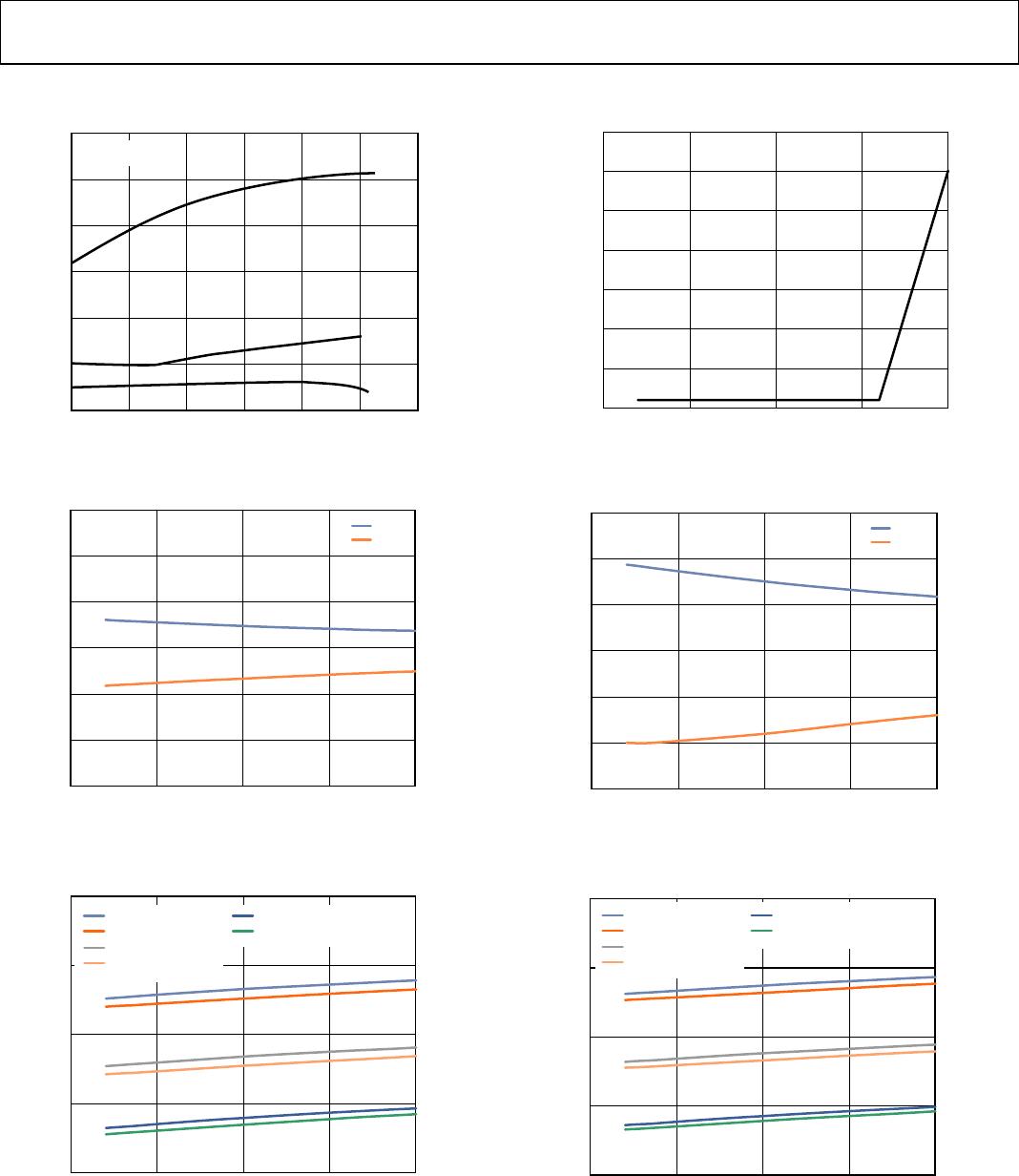
TYPICAL PERFORMANCE CHARACTERISTICS
+85°C
+25°C
–40°C
V
S
= 5V
INPUT COMMON-MODE VOLTAGE (V)
INPUT BIAS CURRENT (pA)
60
40
50
30
10
20
0
0123456
12890-002
Figure 2. Input Bias Current vs. Input Common-Mode Voltage
12890-003
OUTPUT SHORT-CIRCUIT CURRENT (mA)
TEMPERATURE (°C)
–150
–100
–50
0
+50
+100
+150
–75 –25 +25 +75 +125
+I
SC
–I
SC
V
S
= 2.7V
Figure 3. Output Short-Circuit Current vs. Temperature (2.7 V)
12890-004
OUTPUT-TO-RAIL VOLTAGE (mV)
TEMPERATURE (°C)
0.1
1
10
100
1k
–75 –25 +25 +75 +125
V
CC
– V
OH
@ 10k
V
OL
– V
EE
@ 10k
V
CC
– V
OH
@ 1k
V
OL
– V
EE
@ 1k
V
CC
– V
OH
@ 100k
V
OL
– V
EE
@ 100k
V
S
= 2.7V
Figure 4. Output-to-Rail Voltage vs. Temperature (2.7 V)
12890-005
INPUT BIAS CURRENT (pA)
TEMPERATURE (°C)
–75 –25 +25 +75 +125
0
100
200
300
400
500
600
700
V
S
= 5V
Figure 5. Input Bias Current vs. Temperature
12890-006
TEMPERATUREC)
–75 –25 +25 +75 +125
–150
–100
–50
0
+50
+100
+150
OUTPUT SHORT-CIRCUIT CURRENT (mA)
+I
SC
–I
SC
V
S
= 5V
Figure 6. Output Short-Circuit Current vs. Temperature (5 V)
12890-007
OUTPUT-TO-RAIL VOLTAGE (mV)
TEMPERATURE (°C)
0.1
1
10
100
1k
–75 –25 +25 +75 +125
V
S
= 5V
V
CC
– V
OH
@ 10k
V
OL
– V
EE
@ 10k
V
CC
– V
OH
@ 1k
V
OL
– V
EE
@ 1k
V
CC
– V
OH
@ 100k
V
OL
– V
EE
@ 100k
Figure 7. Output-to-Rail Voltage vs. Temperature (5 V)

AD8629TRZ-EP

Mfr. #:
Manufacturer:
Analog Devices Inc.
Description:
Precision Amplifiers DUAL, LOW NOISE AUTO ZERO AMPLIFIER
Lifecycle:
New from this manufacturer.
Delivery:
DHL FedEx Ups TNT EMS
Payment:
T/T Paypal Visa MoneyGram Western Union

Products related to this Datasheet