CY7C199CN
256-Kbit (32 K × 8) Static RAM
Cypress Semiconductor Corporation 198 Champion Court San Jose, CA 95134-1709 408-943-2600
Document Number: 001-06435 Rev. *J Revised January 16, 2015
256-Kbit (32 K × 8) Static RAM
Features
Fast access time: 15 ns
Wide voltage range: 5.0 V ± 10% (4.5 V to 5.5 V)
complementary metal oxide semiconductor (CMOS) for
optimum speed and power
Transistor transistor logic (TTL) compatible inputs and outputs
2.0 V data retention
Low CMOS standby power
Automated power-down when deselected
Available in Pb-free 28-pin molded small outline J-lead (SOJ)
and 28-pin DIP packages
General Description
The CY7C199CN
[1]
is a high performance CMOS Asynchronous
SRAM organized as 32K by 8 bits that supports an asynchronous
memory interface. The device features an automatic
power-down feature that reduces power consumption when
deselected.
See the Truth Table on page 4 in this data sheet for a complete
description of read and write modes.
The CY7C199CN is available in 28-pin molded SOJ and 28-pin
DIP package(s).
For a complete list of related documentation, click here.
Logic Block Diagram
Product Portfolio
Description -15 Unit
Maximum access time 15 ns
Maximum operating current 80 mA
Maximum CMOS standby current (low power) 500 PA
Row Decoder
RAM Array
Column Decoder
Input Buffer
Sense Amps
A
X
Power
Down
Circuit
I/Ox
OE
WE
CE
X
CY7C199CN
Document Number: 001-06435 Rev. *J Page 2 of 17
Contents
Pin Layout and Specifications ........................................3
Pin Description .................................................................3
Truth Table ........................................................................4
Maximum Ratings .............................................................5
Operating Range ...............................................................5
DC Electrical Characteristics ..........................................5
Capacitance ......................................................................6
Thermal Resistance ..........................................................6
AC Test Loads ..................................................................6
AC Test Conditions ..........................................................6
Data Retention Characteristics .......................................7
Data Retention Waveform ................................................7
AC Electrical Characteristics ..........................................8
Ordering Information ......................................................12
Ordering Code Definitions ......................................... 12
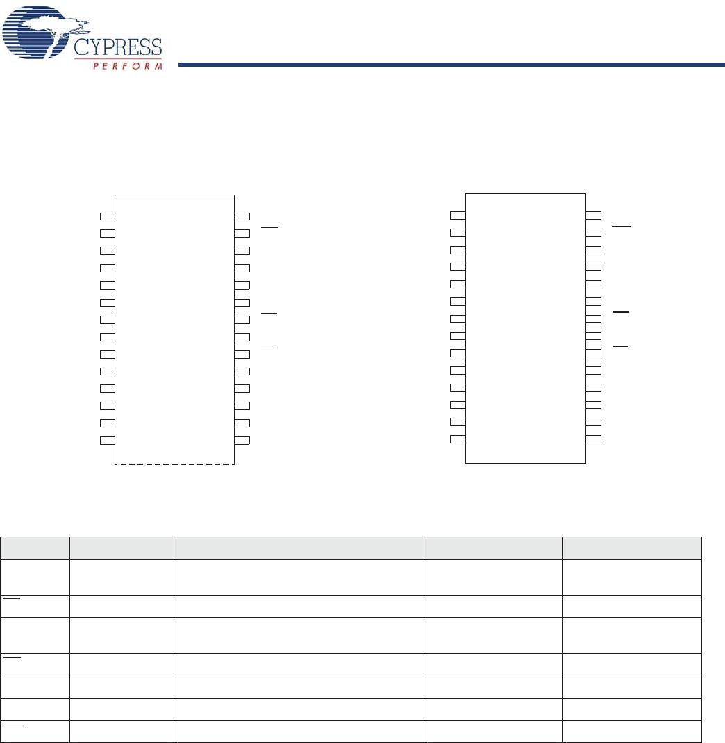
Package Diagrams ..........................................................13
Acronyms ........................................................................15
Document Conventions .................................................15
Units of Measure ....................................................... 15
Document History Page .................................................16
Sales, Solutions, and Legal Information ......................17
Worldwide Sales and Design Support ....................... 17
Products .................................................................... 17
PSoC® Solutions ...................................................... 17
Cypress Developer Community ................................. 17
Technical Support ..................................................... 17
CY7C199CN
Document Number: 001-06435 Rev. *J Page 3 of 17
Pin Layout and Specifications
A
5
A
6
A
7
A
8
A
9
A
10
A
11
A
12
A
13
A
14
IO
0
IO
1
IO
2
V
SS IO
3
IO
4
IO
5
IO
6
IO
7
CE
A
0
OE
A
1
A
2
A
3
A
4
WE
V
CC
1
2
3
4
5
6
7
8
9
10
11
12
13
14 15
16
17
18
19
20
21
22
23
24
25
26
27
28
28-pin DIP
A
5
A
6
A
7
A
8
A
9
A
10
A
11
A
12
A
13
A
14
IO
0
IO
1
IO
2
V
SS
IO
3
IO
4
IO
5
IO
6
IO
7
CE
A
0
OE
A
1
A
2
A
3
A
4
WE
V
CC
1
2
3
4
5
6
7
8
9
10
11
12
13
14
15
16
17
18
19
20
21
22
23
24
25
26
27
28
28-pin SOJ
Pin Description
Pin Type Description DIP SOJ
A
X
Input Address inputs 1, 2, 3, 4, 5, 6, 7, 8, 9, 10,
21, 23, 24, 25, 26
1, 2, 3, 4, 5, 6, 7, 8, 9, 10,
21, 23, 24, 25, 26
CE
Control Chip Enable 20 20
IO
X
Input or Output Data input outputs 11, 12, 13, 15, 16, 17,
18, 19
11, 12, 13, 15, 16, 17,
18, 19
OE
Control Output enable 22 22
V
CC
Supply Power (5.0 V) 28 28
V
SS
Supply Ground 14 14
WE
Control Write Enable 27 27
Note
1. For best practices recommendations, refer to the Cypress application note System Design Guidelines on www.cypress.com.

CY7C199CNL-15VXI

Mfr. #:
Manufacturer:
Cypress Semiconductor
Description:
SRAM 256Kb 15ns 32K x 8 SRAM
Lifecycle:
New from this manufacturer.
Delivery:
DHL FedEx Ups TNT EMS
Payment:
T/T Paypal Visa MoneyGram Western Union

Products related to this Datasheet