AD8346
Rev. A | Page 9 of 20
SB SUPPRESSION (dBc)
–30
–32
–34
–36
–38
–40
–42
–44
05335-019
TEMPERATURE (°C)
40 20 0 20304050607080–30 –10 10
V
P
= 5V
V
P
= 2.7V
V
P
= 3V
V
P
= 5.5V
Figure 19. Sideband Suppression vs. Temperature.
F
LO
= 1900 MHz, I and Q inputs driven in quadrature
with differential amplitude of 2.00 V p-p at F
BB
= 100 kHz.
BASEBAND DIFFERENTIAL INPUT
VOLTAGE (V
p-p)
INPUT THIRD HARMONIC
DISTORTION (dBc)
–30
0.5
–35
–40
–45
–50
–55
1.0 1.5 2.0 2.5 3.0
–60
–65
–70
–75
–80
–6
–8
–10
–12
–14
–16
–18
–20
–22
SSB OUTPUT POWER (dBm)
05335-020
SSB P
OUT
3RD HARMONIC
Figure 20. Third Harmonic Distortion and SSB Output
Power vs. Baseband Differential Input Voltage Level.
F
LO
= 1900 MHz, I and Q inputs driven in quadrature at F
BB
= 100 kHz.
FREQUENCY (MHz)
0
–5
–10
–15
–20
–25
–30
800 1200 1600 2000
–40
RETURN LOSS (dB)
2400
–35
1400 1800 22001000
05335-021
T = –40°C
T = +25°C
T = +85°C
Figure 21. Return Loss of V
OUT
Output vs. F
LO
.
V
POS
= 2.7 V.
BASEBAND FREQUENCY (MHz)
INPUT THIRD HARMONIC
DISTORTION (dB)c
–40
0
–45
–50
–55
–60
–65
2468101214161820
05335-022
V
P
= 5V
V
P
= 5.5V
V
P
= 2.7V
V
P
= 3V
Figure 22. Third Harmonic Distortion vs. F
BB
.
F
LO
=1900 MHz, I and Q inputs driven in quadrature
with differential amplitude of 2.00 V p-p.
52
50
48
46
44
42
40
38
36
SUPPLY CURRENT (mA)
05335-023
TEMPERATURE (°C)
–40 –20 0 20 40 60 80
V
P
= 5V
V
P
= 2.7V
V
P
= 3V
V
P
= 5.5V
Figure 23. Power Supply Current vs. Temperature
FREQUENCY (MHz)
0
–5
–10
–15
–20
–25
–30
800 1200 1600 2000
–40
RETURN LOSS (dB)
2400
–35
1400 1800 22001000
05335-024
T = –40°C
T = +25°C
T = +85°C
Figure 24. Return Loss of V
OUT
Output vs. F
LO
.
V
POS
= 5.0 V.
AD8346
Rev. A | Page 10 of 20
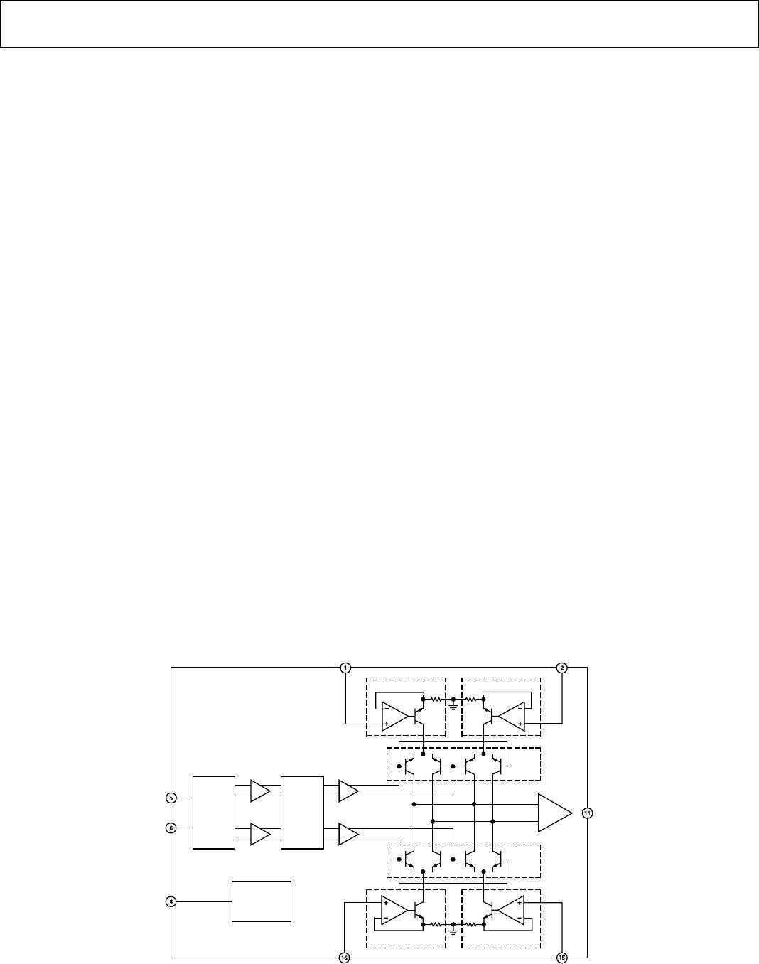
CIRCUIT DESCRIPTION
OVERVIEW
The AD8346 can be divided into the following sections: local
oscillator (LO) interface, mixer, voltage-to-current (V-to-I)
converter, differential-to-single-ended (D-to-S) converter, and
bias. A detailed block diagram of the part is shown in
Figure 25.
The LO interface generates two LO signals, with 90° of phase
difference between them, to drive two mixers in quadrature.
Baseband voltage signals are converted into current form in
the V-to-I converters, feeding into two mixers. The output of
the mixers are combined to feed the D-to-S converter which
provides the 50 Ω output interface. Bias currents to each
section are controlled by the Enable (ENBL) signal. Detailed
descriptions of each section follows.
LO INTERFACE
The differential LO inputs allow the user to drive the LO differ-
entially in order to achieve maximum performance. The LO can
be driven single-endedly but the LO feedthrough performance
is degraded, especially towards the higher end of the frequency
range. The LO interface consists of interleaved stages of
polyphase network phase splitters and buffer amplifiers. The
phase-splitter contains resistors and capacitors connected in a
circular manner to split the LO signal into I and Q paths in
precise quadrature with each other. The signal on each path
goes through a buffer amplifier to make up for the loss and high
frequency roll-off. The two signals then go through another
polyphase network to enhance the quadrature accuracy. The
broad operating frequency range of 0.8 GHz to 2.5 GHz is
achieved by staggering the RC time constants in each stage of
the phase-splitters. The outputs of the second phase-splitter are
fed into the driver amplifiers for the mixers’ LO inputs.
V-TO-I CONVERTER
Each baseband input pin is connected to an op amp driving an
emitter follower. Feedback at the emitter maintains a current
proportional to the input voltage through the transistor. This
current is fed to the two mixers in differential form.
MIXERS
There are two double-balanced mixers, one for the in-phase
channel (I-channel) and one for the quadrature channel
(Q channel). Each mixer uses the gilbert cell design with four
cross-connected transistors. The bases of the transistors are
driven by the LO signal of the corresponding channel. The
output currents from the two mixers are summed together in
two resistors in series with two coupled on-chip inductors. The
signal developed across the R-L loads is sent to the D-to-S stage.
DIFFERENTIAL-TO-SINGLE-ENDED CONVERTER
The differential-to-single-ended converter consists of two
emitter followers driving a totem-pole output stage. Output
impedance is established by the emitter resistors in the output
transistors. The output of this stage is connected to the output
(VOUT) pin.
BIAS
A band gap reference circuit based on the Δ-V
BE
principle
generates the proportional-to-absolute-temperature (PTAT)
currents used by the different sections as references. The band
gap voltage is also used to generate a temperature-stable current
in the V-to-I converters to produce a temperature-independent
slew rate. When the band gap reference is disabled by pulling
down the ENBL pin, all other sections are shut off accordingly.
MIXER
MIXER
V-TO-I
V-TO-I
V-TO-I
V-TO-I
D-TO-S
BIAS CELL
AD8346
LOIN
LOIP
ENBL
QBBP
QBBN
V
OU
T
IBBNIBBP
PHASE
SPLITTER
1
PHASE
SPLITTER
2
05335-025
Figure 25. Detailed Block Diagram
AD8346
Rev. A | Page 11 of 20
BASIC CONNECTIONS
The basic connections for operating the AD8346 are shown in
Figure 27. A single power supply of between 2.7 V and 5.5 V is
applied to pins VPS1 and VPS2. A pair of ESD protection
diodes are connected internally between VPS1 and VPS2 so
these must be tied to the same potential. Both pins should be
individually decoupled using 100 pF and 0.01 μF capacitors,
located as close as possible to the device. For normal operation,
the enable pin, ENBL, must be pulled high. The turn-on
threshold for ENBL is 2 V. To put the device in its power-down
mode, ENBL must be pulled below 0.5 V. Pins COM1 to COM4
should all be tied to a low impedance ground plane.
The I and Q ports should be driven differentially. This is con-
venient as most modern high speed DACs have differential
outputs. For optimal performance, the drive signal should be a
2 V p-p (differential) signal with a bias level of 1.2 V, that is,
each input swings from 0.7 V to 1.7 V. The I and Q inputs have
input impedances of 12 kΩ. By dc coupling the DAC to the
AD8346 and applying small offset voltages, the LO feedthrough
can be reduced to well below its nominal value of −42 dBm
(see
Figure 12).
LO DRIVE
The return loss of the LO port is shown in Figure 18. No add-
itional matching circuitry is required to drive this port from a
50 Ω source. For maximum LO suppression at the output, a
differential LO drive is recommended. In
Figure 27, this is
achieved using a balun (M/A-COM Part Number ETC1-1-13).
The output of the balun is ac-coupled to the LO inputs which
have a bias level about 800 mV below supply. An LO drive
level of between −6 dBm and −12 dBm is required. For optimal
performance, a drive level of −10 dBm is recommended,
although a level of −6 dBm results in more stable temperature
performance (see
Figure 8). Higher levels degrade linearity
while lower levels tend to increase the noise floor.
LOIP
LOIN
AD8346
100pF
100pF
LO
05335-026
Figure 26. Single-Ended LO Drive
The LO terminal can be driven single-ended, as shown in
Figure 26 at the expense of slightly higher LO feedthrough.
LOIN is ac coupled to ground using a capacitor and LOIP is
driven through a coupling capacitor from a (single-ended)
50 Ω source (this scheme could also be reversed with LOIP
being ac-coupled to ground).
RF OUTPUT
The RF output is designed to drive a 50 Ω load, but must be ac-
coupled, as shown in
Figure 27. If the I and Q inputs are driven
in quadrature by 2 V p-p signals, the resulting output power is
about −10 dBm (see
Figure 7 for variations in output power
over frequency).
QBBP
IBBP
AD8346
QBBN
IBBN
COM4
COM1
COM4
COM1
VPS2
LOIN
VOUT
LOIP
COM3
VPS1
COM2
ENBL
1
2
3
4
5
6
7
8
16
15
14
13
12
11
10
9
C4
0.01μF
C3
100pF
C6
100pF
C7
100pF
T1
ETC1-1-13
1
2
3
5
4
C2
0.01μF
C1
100pF
C5
100pF
IP
IN
LO
+V
S
QP
QN
+V
S
VOUT
05335-027
Figure 27. Basic Connections

AD8346ARUZ

Mfr. #:
Manufacturer:
Analog Devices Inc.
Description:
Modulator / Demodulator 2.5GHz Direct Conversion Quadratre
Lifecycle:
New from this manufacturer.
Delivery:
DHL FedEx Ups TNT EMS
Payment:
T/T Paypal Visa MoneyGram Western Union