AD8346
Rev. A | Page 12 of 20
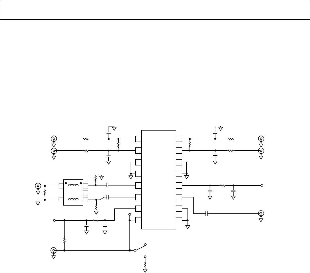
INTERFACE TO AD9761 TXDAC®
Figure 28 shows a dc-coupled current output DAC interface.
The use of dual-integrated DACs, such as the AD9761 with
specified ±0.02 dB and ±0.004 dB gain and offset matching
characteristics, ensures minimum error contribution (over
temperature) from this portion of the signal chain. The use of a
precision thin-film resistor network sets the bias levels precisely
to prevent the introduction of offset errors, which increase LO
feedthrough. For instance, selecting resistor networks with a
0.1% ratio matching characteristics maintains 0.03 dB gain and
offset matching performance.
Using resistive division, the dc bias level at the I and Q inputs
to the AD8346 is set to approximately 1.2 V. Each of the four
current outputs of the DAC delivers a full-scale current of
10 mA, giving a voltage swing of 0 V to 1 V (at the DAC
output). This results in a 0.5 V p-p swing at the I and Q inputs
of the AD8346 (resulting in a 1 V p-p differential swing).
Note that the ratio matching characteristics of the resistive
network, as opposed to its absolute accuracy, is critical in
preserving the gain and offset balance between the I and Q
signal path.
By applying small dc offsets to the I and Q signals from the
DAC, the LO suppression can be reduced from its nominal
value of −42 dBm to as low as −60 dBm while holding to
approximately −50 dBm over temperature (see
Figure 12 for
a plot of LO feedthrough over temperature for an offset
compensated circuit).
I
DAC
2
×
LATCH
I
IOUTB
IOUTA
Q
DAC
2
×
LATCH
Q
QOUTB
QOUTA
MUX
CONTROL
SELECT
WRITE
CLOCK
AD9761
DVDD DCOM AVDD
0.1
μ
F
R
SET
2k
Ω
SLEEP FS ADJ REFIO
DAC
DATA
INPUTS
C
FILTER
100
Ω
100
Ω
C
FILTER
100
Ω
100
Ω
500
Ω
500
Ω
500
Ω
500
Ω
500
Ω
500
Ω
500
Ω
500
Ω
0.1
μ
F
634
Ω
5V
PHASE
SPLITTER
Σ
VOUT
IBBP
IBBN
QBBP
QBBN
AD8346
LOIP
LOIN
VPS1 VPS2
0.5V p-p EACH PIN
WITH V
CM
= 1.2V
+5V
05335-028
Figure 28. AD8346 Interface to AD9761 TxDAC
AD8346
Rev. A | Page 13 of 20
AC-COUPLED INTERFACE
An ac-coupled interface can also be implemented, as shown in
Figure 29. This is an advantage because there is almost no
voltage loss due to the biasing network, allowing the AD8346
inputs to be driven by the full 2 V p-p differential signal from
the AD9761 (each of the DACs 4 outputs delivering 1 V p-p).
As in the dc-coupled case, the bias levels on the I and Q inputs
should be set to as precise a level as possible, relative to each
other. This prevents the introduction of additional input offset
voltages. In
Figure 29, the bias level on each input is set to
approximately 1.2 V. The 2.43 kΩ resistors should have a ratio
tolerance of 0.1% or better.
The network shown has a high-pass corner frequency of
approximately 14.3 kHz (note that the 12 kΩ input impedance
of the AD8346 has been factored into this calculation).
Increasing the resistors in the network or increasing the
coupling capacitance reduces the corner frequency further.
Note that the LO suppression can be manually optimized by
replacing a portion of the four top 2.43 kΩ resistors with
potentiometers. In this case, the bottom four resistors in the
biasing network no longer need to be precision devices.
2 ×
LATCH
I
IOUTB
IOUTA
2 ×
LATCH
Q
QOUTB
QOUTA
MUX
CONTROL
SELECT
WRITE
CLOCK
AD9761
DVDD DCOM AVDD
0.1μF
R
SET
2kΩ
SLEEP FS ADJ REFIO
DAC
DATA
INPUTS
C
FILTER
100Ω
100Ω
C
FILTER
100Ω
100Ω
0.1μF
1kΩ
5V
PHASE
SPLITTER
Σ
VOUT
IBBP
IBBN
QBBP
QBBN
AD8346
LOIP
LOIN
VPS1 VPS2
1V p-p EACH PIN
WITH V
CM
= 1.2V
5V
0.01μF
0.01μF
0.01μF
0.01μF
I
DAC
2.43kΩ
2.43kΩ
2.43kΩ
2.43kΩ
2.43kΩ
2.43kΩ
2.43kΩ
2.43kΩ
Q
DAC
05335-029
Figure 29. AC-Coupled DAC Interface
AD8346
Rev. A | Page 14 of 20
EVALUATION BOARD
The schematic of the AD8346 evaluation board is shown in
Figure 30. This is a 4-layer FR4 board; the two center layers are
used as ground planes and the top and bottom layers are used
for signal and power.
Figure 31 shows the layout and Figure 32
shows the silkscreen. The evaluation board circuit closely
follows the basic connections circuit shown in
Figure 27.
Slide SW1 to the A position to connect the ENBL pin to +V
S
via the 10 kΩ pull-up resistor REP. Slide SW1 to the B position
to disable the device by grounding the ENOP pin through the
49.9 Ω pull-down resistor REG. The device may be enabled via
an external voltage applied to the SMA connector ENOP or TP2.
All connectors are of the SMA type. The I and Q inputs are
provided with pads for implementing a simple RC filter
network. The local oscillator input is driven through a balun
(M/A-COM Part Number ETC1-1-13).
05335-030
C4
100pF
C3
0.01
μ
F
QP
QN
CLOP
100pF
CLON
100pF
LO
RLOP
OPEN
RLON
OPEN
RLOS
OPEN
1
2
3
4
5
6
7
8
16
15
14
13
12
10
9
11
IBBP
IBBN
COM1
COM1
LOIN
LOIP
VPS1
ENBL
QBBP
QBBN
COM4
COM4
VPS2
VOUT
COM3
COM2
TP2
ENOP
IP
IN
ENOP
CVO
100pF
VOUT
+V
S
+V
S
AD8346
RQP
0
Ω
CQP
OPEN
RQN
0
Ω
R2
0
Ω
CIP
OPEN
RIP
0
Ω
RIN
0
Ω
CIN
OPEN
C1
0.01
μ
F
C2
100pF
R7
0
Ω
T1
ETC1-1-13
1
2
3
5
4
RIS
OPEN
RQS
OPEN
CQN
OPEN
REG
49.9k
Ω
REP
10k
Ω
A
B
SW1
Figure 30. Evaluation Board Schematic

AD8346ARUZ

Mfr. #:
Manufacturer:
Analog Devices Inc.
Description:
Modulator / Demodulator 2.5GHz Direct Conversion Quadratre
Lifecycle:
New from this manufacturer.
Delivery:
DHL FedEx Ups TNT EMS
Payment:
T/T Paypal Visa MoneyGram Western Union