Data Sheet ADuM2200/ADuM2201
Rev. G | Page 13 of 17
APPLICATIONS INFORMATION
PCB LAYOUT
The ADuM2200/ADuM2201 digital isolators require no external
interface circuitry for the logic interfaces. Power supply bypassing
is strongly recommended at the input and output supply pins (see
Figure 12). Bypass capacitors are most conveniently connected
between Pin 1 and Pin 3 for V
DD1
and between Pin 14 and Pin 16
for V
DD2
. The capacitor value should be between 0.01 μF and 0.1 μF.
The total lead length between both ends of the capacitor and the
input power supply pin should not exceed 2 mm. Consider
bypassing between Pin 3 and Pin 7 and between Pin 9 and Pin 14
unless the ground pair on each package side is connected close
to the package.
GND
1
NC
V
DD1
V
IA
/V
OA
GND
2
NC
V
DD2
V
OA
/V
IA
V
IB
V
OB
NC
NC
GND
1
NC
NC
GND
2
07235-012
Figure 12. Recommended Printed Circuit Board Layout
In applications involving high common-mode transients, ensure
that board coupling across the isolation barrier is minimized.
Furthermore, design the board layout such that any coupling that
does occur affects all pins equally on a given component side.
Failure to ensure this can cause voltage differentials between
pins exceeding the absolute maximum ratings for the device as
specified in Table 18, thereby leading to latch-up or permanent
damage.
See the AN-1109 Application Note for board layout guidelines.
PROPAGATION DELAY-RELATED PARAMETERS
Propagation delay is a parameter that describes the length of
time it takes for a logic signal to propagate through a component.
The propagation delay to a logic low output can differ from the
propagation delay to a logic high output.
INPUT (
V
Ix
)
OUTPUT (V
Ox
)
t
PLH
t
PHL
50%
50%
07235-018
Figure 13. Propagation Delay Parameters
Pulse width distortion is the maximum difference between
these two propagation delay values and is an indication of how
accurately the timing of the input signal is preserved.
Channel-to-channel matching refers to the maximum amount
that the propagation delay differs between channels within a
single ADuM2200/ADuM2201 component.
Propagation delay skew refers to the maximum amount that
the propagation delay differs between multiple ADuM2200/
ADuM2201 components operated under the same conditions.
DC CORRECTNESS AND MAGNETIC FIELD
IMMUNITY
Positive and negative logic transitions at the isolator input cause
narrow (~1 ns) pulses to be sent to the decoder via the transformer.
The decoder is bistable and is, therefore, either set or reset by
the pulses, indicating input logic transitions. In the absence of
logic transitions at the input for more than ~1 μs, a periodic set
of refresh pulses indicative of the correct input state is sent to
ensure dc correctness at the output. If the decoder receives no
internal pulses for more than approximately 5 μs, the input side
is assumed to be unpowered or nonfunctional, and the isolator
output is forced to a default state by the watchdog timer circuit
(see Table 20 and Table 21).
The limitation on the magnetic field immunity of the ADuM2200/
ADuM2201 is set by the condition in which induced voltage in the
transformer receiving coil is large enough to either falsely set or
reset the decoder. The following analysis defines the conditions
under which this can occur. The 3.3 V operating condition of
the ADuM2200/ADuM2201 is examined because it represents
the most susceptible mode of operation.
The pulses at the transformer output have an amplitude greater
than 1.0 V. The decoder has a sensing threshold at approximately
0.5 V, thus establishing a 0.5 V margin in which induced voltages
can be tolerated. The voltage induced across the receiving coil is
given by
V = (−dβ/dt) ∑ πr
n
2
; n = 1, 2, … , N
where:
β is the magnetic flux density (gauss).
r
n
is the radius of the n
th
turn in the receiving coil (cm).
N is the number of turns in the receiving coil.
Given the geometry of the receiving coil in the ADuM2200/
ADuM2201 and an imposed requirement that the induced
voltage be, at most, 50% of the 0.5 V margin at the decoder,
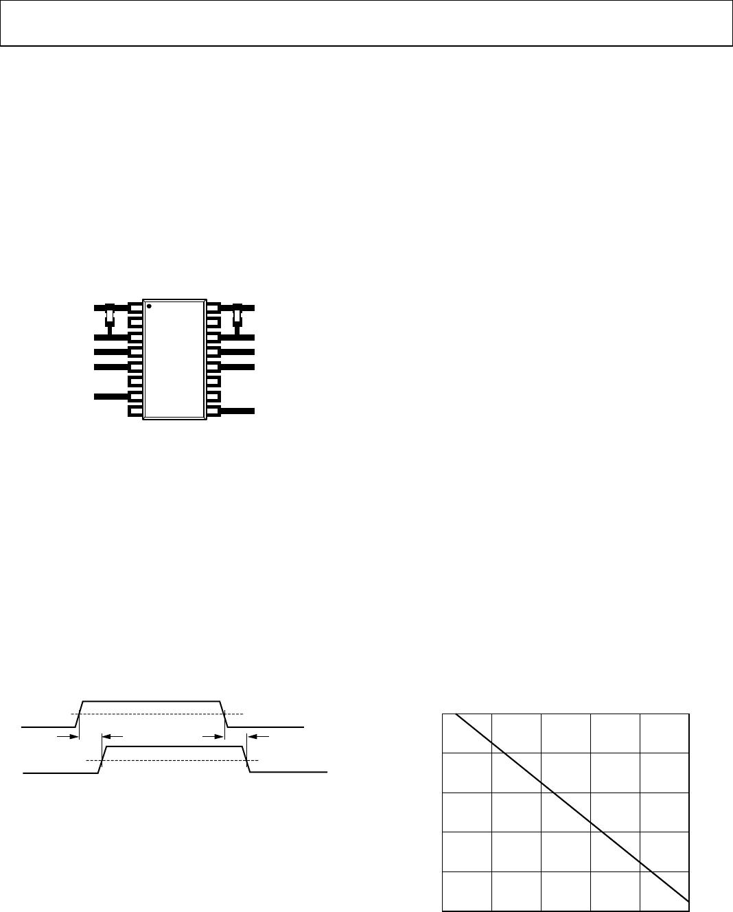
a maximum allowable magnetic field is calculated as shown
in Figure 14.
MAGNETIC FIELD FREQUENCY (Hz)
100
MAXIMUM ALLOWABLE MAGNETIC FLUX
DENSITY (kgauss)
0.001
1M
10
0.01
1k 10k 10M
0.1
1
100M100k
07235-019
Figure 14. Maximum Allowable External Magnetic Flux Density
ADuM2200/ADuM2201 Data Sheet
Rev. G | Page 14 of 17
For example, at a magnetic field frequency of 1 MHz, the
maximum allowable magnetic field of 0.2 kgauss induces a voltage
of 0.25 V at the receiving coil. This voltage is approximately
50% of the sensing threshold and does not cause a faulty output
transition. Similarly, if such an event occurs during a transmitted
pulse (and is of the worst-case polarity), it reduces the received
pulse from >1.0 V to 0.75 V—still well above the 0.5 V sensing
threshold of the decoder.
The preceding magnetic flux density values correspond to
specific current magnitudes at given distances from the
ADuM2200/ADuM2201 transformers. Figure 15 expresses
these allowable current magnitudes as a function of frequency
for selected distances. As shown in Figure 15, the ADuM2200/
ADuM2201 are immune and can be affected only by extremely
large currents operated at high frequency very close to the
component. For the 1 MHz example noted, a 0.5 kA current
placed 5 mm away from the ADuM2200/ADuM2201 is
required to affect the operation of the component.
MAGNETIC FIELD FREQUENCY (Hz)
MAXIMUM ALLOWABLE CURRENT (kA)
1000
100
10
1
0.1
0.01
1k 10k 100M100k 1M 10M
DISTANCE = 5mm
DISTANCE = 1m
DISTANCE = 100mm
07235-020
Figure 15. Maximum Allowable Current
for Various Current-to-ADuM2200/ADuM2201 Spacings
Note that at combinations of strong magnetic field and high
frequency, any loops formed by printed circuit board traces can
induce error voltages sufficiently large to trigger the thresholds
of succeeding circuitry. Care should be taken in the layout of
such traces to avoid this possibility.
POWER CONSUMPTION
The supply current at a given channel of the ADuM2200/
ADuM2201 isolators is a function of the supply voltage, the
channel data rate, and the channel output load.
For each input channel, the supply current is given by
I
DDI
= I
DDI (Q)
f ≤ 0.5f
r
I
DDI
= I
DDI (D)
× (2f − f
r
) + I
DDI (Q)
f > 0.5f
r
For each output channel, the supply current is given by
I
DDO
= I
DDO (Q)
f ≤ 0.5f
r
I
DDO
= (I
DDO (D)
+ (0.5 × 10
−3
) × C
L
× V
DDO
) × (2ff
r
) + I
DDO (Q)
f > 0.5f
r
where:
I
DDI (D)
, I
DDO (D)
are the input and output dynamic supply currents
per channel (mA/Mbps).
I
DDI (Q)
, I
DDO (Q)
are the specified input and output quiescent
supply currents (mA).
C
L
is the output load capacitance (pF).
V
DDO
is the output supply voltage (V).
f is the input logic signal frequency (MHz, half of the input data
rate, NRZ signaling).
f
r
is the input stage refresh rate (Mbps).
To calculate the total I
DD1
and I
DD2
, the supply currents for each
input and output channel corresponding to I
DD1
and I
DD2
are
calculated and totaled.
Figure 6 and Figure 7 provide per-channel supply currents as a
function of data rate for an unloaded output condition. Figure 8
provides per-channel supply current as a function of data rate for
a 15 pF output condition. Figure 9 through Figure 11 provide total
I
DD1
and I
DD2
as a function of data rate for the ADuM2200/
ADuM2201 channel configurations.
Data Sheet ADuM2200/ADuM2201
Rev. G | Page 15 of 17
INSULATION LIFETIME
All insulation structures eventually break down when subjected
to voltage stress over a sufficiently long period. The rate of
insulation degradation is dependent on the characteristics of the
voltage waveform applied across the insulation. In addition to the
testing performed by the regulatory agencies, Analog Devices
carries out an extensive set of evaluations to determine the
lifetime of the insulation structure within the ADuM2200/
ADuM2201 devices.
Analog Devices performs accelerated life testing using voltage
levels higher than the rated continuous working voltage.
Acceleration factors for several operating conditions are
determined. These factors allow calculation of the time to failure
at the actual working voltage.
The values shown in Table 19 summarize the peak voltage for
50 years of service life for a bipolar ac operating condition and
the maximum CSA/VDE approved working voltages. In many
cases, the approved working voltage is higher than the 50-year
service life voltage. Operation at these high working voltages
can lead to shortened insulation life in some cases.
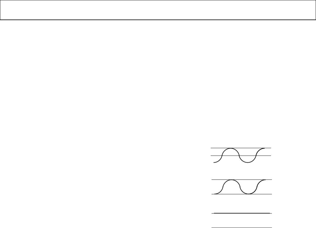
The insulation lifetime of the ADuM2200/ADuM2201 depends
on the voltage waveform type imposed across the isolation barrier.
The iCoupler insulation structure degrades at different rates,
depending on whether the waveform is bipolar ac, unipolar ac,
or dc. Figure 16, Figure 17, and Figure 18 illustrate these
different isolation voltage waveforms.
Bipolar ac voltage is the most stringent environment. The goal
of a 50-year operating lifetime under the bipolar ac condition
determines the maximum working voltage recommended by
Analog Devices.
In the case of unipolar ac or dc voltage, the stress on the insulation
is significantly lower. This allows operation at higher working
voltages while still achieving a 50-year service life. The working
voltages listed in Table 19 can be applied while maintaining the
50-year minimum lifetime, provided that the voltage conforms
to either the unipolar ac or dc voltage cases.
Any cross-insulation voltage waveform that does not conform to
Figure 17 or Figure 18 should be treated as a bipolar ac waveform
and its peak voltage should be limited to the 50-year lifetime
voltage value listed in Table 19.
Note that the voltage presented in Figure 17 is shown as sinusoidal
for illustration purposes only. It is meant to represent any voltage
waveform varying between 0 V and some limiting value. The
limiting value can be positive or negative, but the voltage cannot
cross 0 V.
0V
RATED PEAK VOLTAGE
07235-021
Figure 16. Bipolar AC Waveform
0V
RATED PEAK VOLTAGE
07235-022
Figure 17. Unipolar AC Waveform
0V
RATED PEAK VOLTAGE
07235-023
Figure 18. DC Waveform

ADUM2201BRIZ-RL

Mfr. #:
Manufacturer:
Analog Devices Inc.
Description:
Digital Isolators Dual-CH Digital 5kV
Lifecycle:
New from this manufacturer.
Delivery:
DHL FedEx Ups TNT EMS
Payment:
T/T Paypal Visa MoneyGram Western Union