TLP266J
3
7.
7.
7.
7. Absolute Maximum Ratings (Note) (Unless otherwise specified, T
Absolute Maximum Ratings (Note) (Unless otherwise specified, T
Absolute Maximum Ratings (Note) (Unless otherwise specified, T
Absolute Maximum Ratings (Note) (Unless otherwise specified, T
a
a
a
a
= 25
= 25
= 25
= 25
)
)
)
)
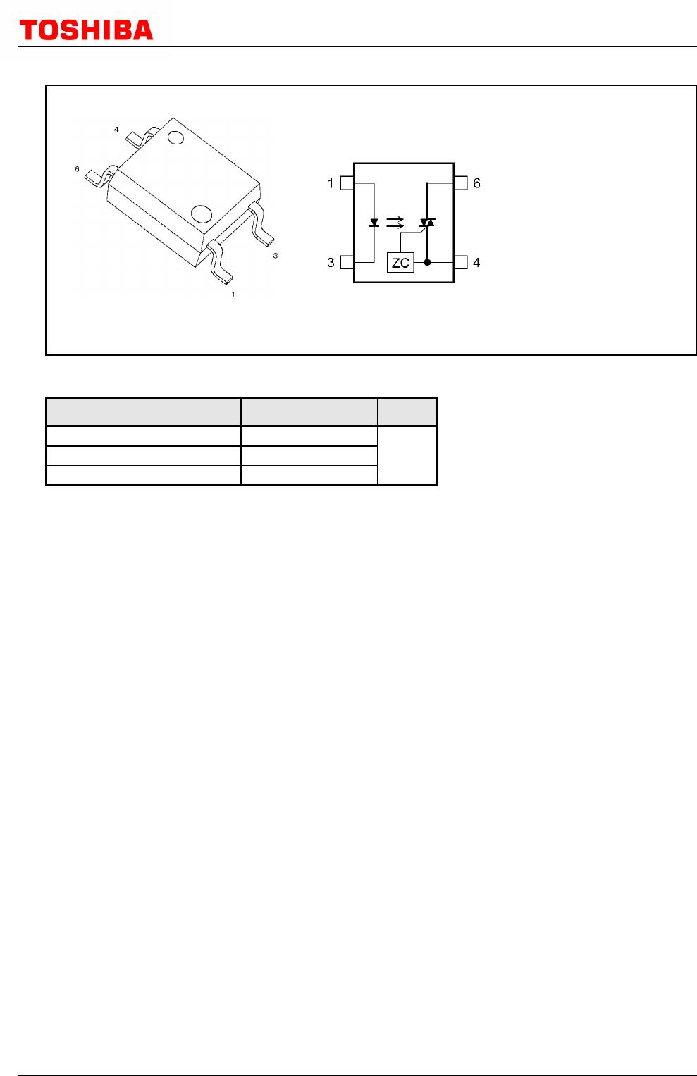
LED
Detector
Common
Characteristics
Input forward current
Input forward current derating
Input forward current (pulsed)
Input reverse voltage
Junction temperature
Input power dissipation
Off-state output terminal voltage
R.M.S. on-state current
R.M.S. on-state current
R.M.S. on-state current derating
ON-state current (pulsed)
Peak non-repetitive surge current
Junction temperature
Output power dissipation
Operating temperature
Storage temperature
Lead soldering temperature
Isolation voltage
(T
a
≥ 53 )
(T
a
= 25 )
(T
a
= 70 )
(T
a
≥ 25 )
(10 s)
AC, 60 s, R.H. ≤ 60 %
Symbol
I
F
∆I
F
/∆T
a
I
FP
V
R
T
j
P
D
V
DRM
I
T(RMS)
I
T(RMS)
∆I
T(RMS)
/∆T
a
I
ONP
I
TSM
T
j
P
O
T
opr
T
stg
T
sol
BV
S
Note
(Note 1)
(Note 2)
(Note 3)
(Note 4)
Rating
50
-0.7
1
5
125
50
600
70
40
-0.67
2
1.2
125
200
-40 to 100
-55 to 125
260
3750
Unit
mA
mA/
A
V
mW
V
mA
mA/
A
A
mW
Vrms
Note: Using continuously under heavy loads (e.g. the application of high temperature/current/voltage and the
significant change in temperature, etc.) may cause this product to decrease in the reliability significantly even
if the operating conditions (i.e. operating temperature/current/voltage, etc.) are within the absolute maximum
ratings.
Please design the appropriate reliability upon reviewing the Toshiba Semiconductor Reliability Handbook
("Handling Precautions"/"Derating Concept and Methods") and individual reliability data (i.e. reliability test
report and estimated failure rate, etc).
Note 1: Pulse width (PW) ≤ 100 µs, 100 pps
Note 2: Pulse width (PW) ≤ 100 µs, 120 pps
Note 3: Pulse width (PW) ≤ 10 ms
Note 4: This device is considered as a two-terminal device: Pins 1 and 3 are shorted together, and pins 4 and 6 are
shorted together.
8.
8.
8.
8. Recommended Operating Conditions (Note)
Recommended Operating Conditions (Note)
Recommended Operating Conditions (Note)
Recommended Operating Conditions (Note)
Characteristics
AC mains voltage
Input forward current
ON-state current (pulsed)
Operating temperature
Symbol
V
AC
I
F
I
ONP
T
opr
Note Min
15
-25
Typ.
20
Max
240
25
1
85
Unit
V
mA
A
Note: Using continuously under heavy loads (e.g. the application of high temperature/current/voltage and the
significant change in temperature, etc.) may cause this product to decrease in the reliability significantly even
if the operating conditions (i.e. operating temperature/current/voltage, etc.) are within the absolute maximum
ratings.
Please design the appropriate reliability upon reviewing the Toshiba Semiconductor Reliability Handbook
("Handling Precautions"/"Derating Concept and Methods") and individual reliability data (i.e. reliability test
report and estimated failure rate, etc).
2017-04-18
Rev.6.0