TLP266J
4
9.
9.
9.
9. Electrical Characteristics (Unless otherwise specified, T
Electrical Characteristics (Unless otherwise specified, T
Electrical Characteristics (Unless otherwise specified, T
Electrical Characteristics (Unless otherwise specified, T
a
a
a
a
= 25
= 25
= 25
= 25
)
)
)
)
LED
Detector
Characteristics
Input forward voltage
Input reverse current
Input capacitance
Peak off-state current
Peak on-state voltage
Holding current
Critical rate of rise of off-state
voltage
Critical rate of rise of
commutating voltage (dv/dt)
Symbol
V
F
I
R
C
t
I
DRM
V
TM
I
H
dv/dt
dv/dt(c)
Note Test Condition
I
F
= 10 mA
V
R
= 5 V
V = 0 V, f = 1 MHz
V
DRM
= 600 V
I
TM
= 70 mA
V
in
= 240 V, T
a
= 85
See Fig. 9.1.
V
in
= 60 Vrms, I
T
= 15 mA
See Fig. 9.1.
Min
1.0
200
Typ.
1.27
30
10
1.7
0.6
500
0.2
Max
1.4
10
1000
2.8
Unit
V
µA
pF
nA
V
mA
V/µs
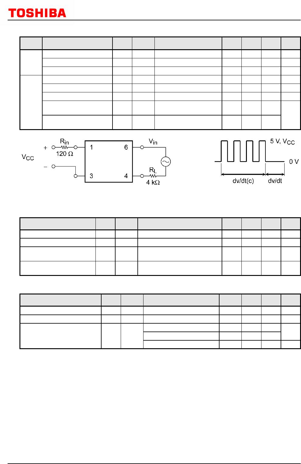
Fig.
Fig.
Fig.
Fig. 9.1
9.1
9.1
9.1 dv/dt Test Circuit
dv/dt Test Circuit
dv/dt Test Circuit
dv/dt Test Circuit
10.
10.
10.
10. Coupled Electrical Characteristics (Unless otherwise specified, T
Coupled Electrical Characteristics (Unless otherwise specified, T
Coupled Electrical Characteristics (Unless otherwise specified, T
Coupled Electrical Characteristics (Unless otherwise specified, T
a
a
a
a
= 25
= 25
= 25
= 25
)
)
)
)
Characteristics
Trigger LED current
Inhibit voltage
Inhibit current
Turn-on time
Symbol
I
FT
V
IH
I
IH
t
on
Note Test Condition
V
T
= 3 V
I
F
= Rated I
FT
I
F
= Rated I
FT
V
T
= Rated V
DRM
V
D
= 6 → 4 V, R
L
= 100 Ω,
I
F
= Rated I
FT
× 1.5 mA
Min
Typ.
200
30
Max
10
30
600
100
Unit
mA
V
µA
µs
11.
11.
11.
11. Isolation Characteristics (Unless otherwise specified, T
Isolation Characteristics (Unless otherwise specified, T
Isolation Characteristics (Unless otherwise specified, T
Isolation Characteristics (Unless otherwise specified, T
a
a
a
a
= 25
= 25
= 25
= 25
)
)
)
)
Characteristics
Total capacitance (input to output)
Isolation resistance
Isolation voltage
Symbol
C
S
R
S
BV
S
Note
(Note 1)
(Note 1)
(Note 1)
Test Condition
V
S
= 0 V, f = 1 MHz
V
S
= 500 V, R.H. ≤ 60%
AC, 60 s
AC, 1 s in oil
DC, 60 s, in oil
Min
1 × 10
12
3750
Typ.
0.8
10
14
10000
10000
Max
Unit
pF
Ω
Vrms
Vdc
Note 1: This device is considered as a two-terminal device: Pins 1 and 3 are shorted together, and pins 4 and 6 are
shorted together.
2017-04-18
Rev.6.0

