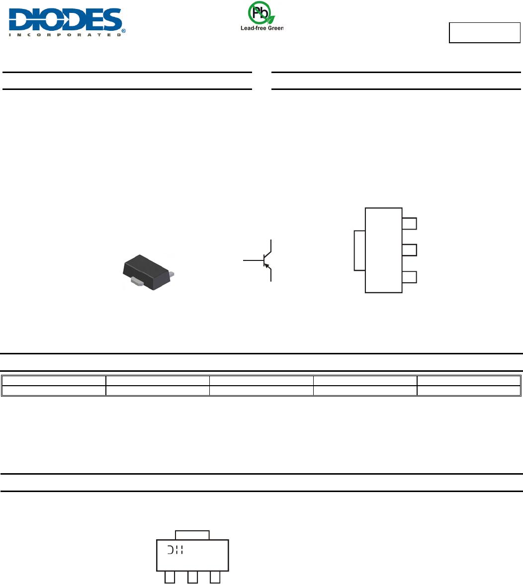
2DB1697
Document number: DS31618 Rev. 3 - 2
2 of 5
www.diodes.com
April 2012
© Diodes Incorporated
2DB1697
NEW PRODUCT
Maximum Ratings @T
A
= 25°C unless otherwise specified
Characteristic Symbol Value Unit
Collector-Base Voltage
V
CBO
-15 V
Collector-Emitter Voltage
V
CEO
-12 V
Emitter-Base Voltage
V
EBO
-6 V
Peak Pulse Current
I
CM
-4 A
Continuous Collector Current
I
C
-2 A
Thermal Characteristics @T
A
= 25°C unless otherwise specified
Characteristic Symbol Value Unit
Power Dissipation (Note 4)
P
D
0.9 W
Thermal Resistance, Junction to Ambient Air (Note 4)
R
JA
139 °C/W
Power Dissipation (Note 5)
P
D
2 W
Thermal Resistance, Junction to Ambient Air (Note 5)
R
JA
62.5 °C/W
Operating and Storage Temperature Range
T
J
, T
STG
-55 to +150 °C
Electrical Characteristics @T
A
= 25°C unless otherwise specified
Characteristic Symbol Min Typ Max Unit Conditions
OFF CHARACTERISTICS
Collector-Base Breakdown Voltage
V
BR
CBO
-15
⎯ ⎯
V
I
C
= -100μA, I
E
= 0
Collector-Emitter Breakdown Voltage (Note 6)
V
BR
CEO
-12
⎯ ⎯
V
I
C
= -10mA, I
B
= 0
Emitter-Base Breakdown Voltage
V
BR
EBO
-6
⎯ ⎯
V
I
E
= -100μA, I
C
= 0
Collector Cut-Off Current
I
CBO
⎯ ⎯
-0.1
μA
V
CB
= -15V, I
E
= 0
Emitter Cut-Off Current
I
EBO
⎯ ⎯
-0.1
μA
V
EB
= -6V, I
C
= 0
ON CHARACTERISTICS (Note 6)
Collector-Emitter Saturation Voltage
V
CE
SAT
⎯
-65 -180 mV
I
C
= -1A, I
B
= -50mA
DC Current Gain
h
FE
270
⎯
680
⎯
V
CE
= -2V, I
C
= -200mA
SMALL SIGNAL CHARACTERISTICS
Output Capacitance
C
obo
⎯
40
⎯
pF
V
CB
= -10V, I
E
= 0,
f = 1MHz
Current Gain-Bandwidth Product
f
T
⎯
140
⎯
MHz
V
CE
= -2V, I
C
= -100mA,
f = 100MHz
Notes: 4. Device mounted on FR-4 PCB with minimum recommended pad layout.
5. Device mounted on FR-4 PCB with 1 inch
2
copper pad layout.
6. Measured under pulsed conditions. Pulse width = 300μs. Duty cycle ≤2%.