CAT1021, CAT1022, CAT1023
www.onsemi.com
4
Table 4. CAT102X FAMILY OVERVIEW
Device Manual Reset
Input Pin
Watchdog Watchdog
Monitor Pin
Write
Protection
Pin
Independent
Auxiliary Voltage
Sense
RESET:
Active High
and LOW
EEPROM
CAT1021
n n
SDA
n n
2k
CAT1022
n n
SDA 2k
CAT1023
n n
WDI
n
2k
CAT1024
n
2k
CAT1025
n n n
2k
CAT1026
n n
2k
CAT1027
n
WDI
n
2k
NOTE: Device will meet the specifications after thermal equilibrium has been established when mounted in a test socket or printed circuit
board with maintained transverse airflow greater than 500 lfpm.
SPECIFICATIONS
Table 5. ABSOLUTE MAXIMUM RATINGS
Parameters Ratings Units
Temperature Under Bias –55 to +125 °C
Storage Temperature –65 to +150 °C
Voltage on any Pin with Respect to Ground (Note 1) 2.0 to V
CC
+ 2.0 V
V
CC
with Respect to Ground 2.0 to 7.0 V
Package Power Dissipation Capability (T
A
= 25°C) 1.0 W
Lead Soldering Temperature (10 s) 300 °C
Output Short Circuit Current (Note 2) 100 mA
Stresses exceeding those listed in the Maximum Ratings table may damage the device. If any of these limits are exceeded, device functionality
should not be assumed, damage may occur and reliability may be affected.
1. The minimum DC input voltage is –0.5 V. During transitions, inputs may undershoot to –2.0 V for periods of less than 20 ns. Maximum
DC voltage on output pins is V
CC
+0.5 V, which may overshoot to V
CC
+2.0 V for periods of less than 20 ns.
2. Output shorted for no more than one second. No more than one output shorted at a time.
Table 6. D.C. OPERATING CHARACTERISTICS
V
CC
= 2.7 V to 5.5 V and over the recommended temperature conditions unless otherwise specified.
Symbol
Parameter Test Conditions Min Typ Max Units
I
LI
Input Leakage Current V
IN
= GND to V
CC
2 10
mA
I
LO
Output Leakage Current V
IN
= GND to V
CC
10 10
mA
I
CC1
Power Supply Current (Write) f
SCL
= 400 kHz
V
CC
= 5.5 V
3 mA
I
CC2
Power Supply Current (Read) f
SCL
= 400 kHz
V
CC
= 5.5 V
1 mA
I
SB
Standby Current V
CC
= 5.5 V
V
IN
= GND to V
CC
60
mA
V
IL
(Note 3) Input Low Voltage 0.5 0.3 x V
CC
V
V
IH
(Note 3) Input High Voltage 0.7 x V
CC
V
CC
+ 0.5 V
V
OL
Output Low Voltage
(SDA, RESET)
I
OL
= 3 mA
V
CC
= 2.7 V
0.4 V
V
OH
Output High Voltage
(RESET)
I
OH
= 0.4 mA
V
CC
= 2.7 V
V
CC
0.75 V
CAT1021, CAT1022, CAT1023
www.onsemi.com
5
Table 6. D.C. OPERATING CHARACTERISTICS
V
CC
= 2.7 V to 5.5 V and over the recommended temperature conditions unless otherwise specified.
Symbol UnitsMaxTypMinTest ConditionsParameter
V
TH
Reset Threshold
CAT102x45
(V
CC
= 5.0 V)
4.50 4.75
V
CAT102x42
(V
CC
= 5.0 V)
4.25 4.50
CAT102x30
(V
CC
= 3.3 V)
3.00 3.15
CAT102x28
(V
CC
= 3.3 V)
2.85 3.00
CAT102x25
(V
CC
= 3.0 V)
2.55 2.70
V
RVALID
Reset Output Valid V
CC
Voltage 1.00 V
V
RT
(Note 4) Reset Threshold Hysteresis 15 mV
3. V
IL
min and V
IH
max are reference values only and are not tested.
4. This parameter is tested initially and after a design or process change that affects the parameter. Not 100% tested.
Table 7. CAPACITANCE
T
A
= 25°C, f = 1.0 MHz, V
CC
= 5 V
Symbol Test Test Conditions Max Units
C
OUT
(Note 5) Output Capacitance V
OUT
= 0 V 8 pF
C
IN
(Note 5) Input Capacitance V
IN
= 0 V 6 pF
Table 8. AC CHARACTERISTICS
V
CC
= 2.7 V to 5.5 V and over the recommended temperature conditions, unless otherwise specified.
Memory Read & Write Cycle (Note 6)
Symbol
Parameter Min Max Units
f
SCL
Clock Frequency 400 kHz
t
SP
Input Filter Spike Suppression (SDA, SCL) 100 ns
t
LOW
Clock Low Period 1.3
ms
t
HIGH
Clock High Period 0.6
ms
t
R
(Note 5) SDA and SCL Rise Time 300 ns
t
F
(Note 5) SDA and SCL Fall Time 300 ns
t
HD;
STA
Start Condition Hold Time 0.6
ms
t
SU;
STA
Start Condition Setup Time (for a Repeated Start) 0.6
ms
t
HD;
DAT
Data Input Hold Time 0 ns
t
SU;
DAT
Data Input Setup Time 100 ns
t
SU;
STO
Stop Condition Setup Time 0.6
ms
t
AA
SCL Low to Data Out Valid 900 ns
t
DH
Data Out Hold Time 50 ns
t
BUF
(Note 5) Time the Bus must be Free Before a New Transmission Can Start 1.3
ms
t
WC
(Note 7) Write Cycle Time (Byte or Page) 5 ms
5. This parameter is characterized initially and after a design or process change that affects the parameter. Not 100% tested.
6. Test Conditions according to “AC Test Conditions” table.
7. The write cycle time is the time from a valid stop condition of a write sequence to the end of the internal program/erase cycle. During the
write cycle, the bus interface circuits are disabled, SDA is allowed to remain high and the device does not respond to its slave address.
CAT1021, CAT1022, CAT1023
www.onsemi.com
6
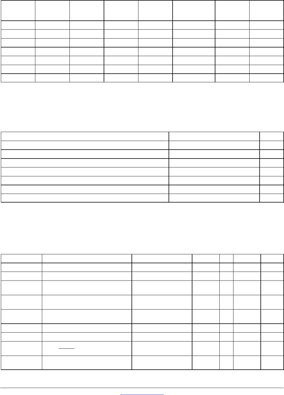
Table 9. RESET CIRCUIT AC CHARACTERISTICS
Symbol Parameter Test Conditions Min Typ Max Units
t
PURST
PowerUp Reset Timeout Note 2 130 200 270 ms
t
RDP
V
TH
to RESET output Delay Note 3 5
ms
t
GLITCH
V
CC
Glitch Reject Pulse Width Notes 4 and 5 30 ns
MR Glitch Manual Reset Glitch Immunity Note 1 100 ns
t
MRW
MR Pulse Width Note 1 5
ms
t
MRD
MR Input to RESET Output Delay Note 1 1
ms
t
WD
Watchdog Timeout Note 1 1.0 1.6 2.1 sec
Table 10. POWERUP TIMING (Notes 5 and 6)
Symbol Parameter Test Conditions Min Typ Max Units
t
PUR
PowerUp to Read Operation 270 ms
t
PUW
PowerUp to Write Operation 270 ms
Table 11. AC TEST CONDITIONS
Parameter Test Conditions
Input Pulse Voltages 0.2 x V
CC
to 0.8 x V
CC
Input Rise and Fall Times 10 ns
Input Reference Voltages 0.3 x V
CC
, 0.7 x V
CC
Output Reference Voltages 0.5 x V
CC
Output Load Current Source: I
OL
= 3 mA; C
L
= 100 pF
Table 12. RELIABILITY CHARACTERISTICS
Symbol Parameter Reference Test Method Min Max Units
N
END
(Note 5) Endurance MILSTD883, Test Method 1033 1,000,000 Cycles/Byte
T
DR
(Note 5) Data Retention MILSTD883, Test Method 1008 100 Years
V
ZAP
(Note 5) ESD Susceptibility MILSTD883, Test Method 3015 2000 Volts
I
LTH
(Notes 5 & 7) LatchUp JEDEC Standard 17 100 mA
1. Test Conditions according to “AC Test Conditions” table.
2. Powerup, Input Reference Voltage V
CC
= V
TH
, Reset Output Reference Voltage and Load according to “AC Test Conditions” Table
3. PowerDown, Input Reference Voltage V
CC
= V
TH
, Reset Output Reference Voltage and Load according to “AC Test Conditions” Table
4. V
CC
Glitch Reference Voltage = V
THmin
; Based on characterization data
5. This parameter is characterized initially and after a design or process change that affects the parameter. Not 100% tested.
6. t
PUR
and t
PUW
are the delays required from the time V
CC
is stable until the specified memory operation can be initiated.
7. Latchup protection is provided for stresses up to 100 mA on input and output pins from 1 V to V
CC
+ 1 V.

CAT1022YI-25-GT3

Mfr. #:
Manufacturer:
ON Semiconductor
Description:
Supervisory Circuits CPU SUP W/2K EEPROM
Lifecycle:
New from this manufacturer.
Delivery:
DHL FedEx Ups TNT EMS
Payment:
T/T Paypal Visa MoneyGram Western Union