LTM8057
7
8057f
For more information www.linear.com/LTM8057
TYPICAL PERFORMANCE CHARACTERISTICS
Unless otherwise noted, operating conditions are
as in Table 1 (T
A
= 25°C).
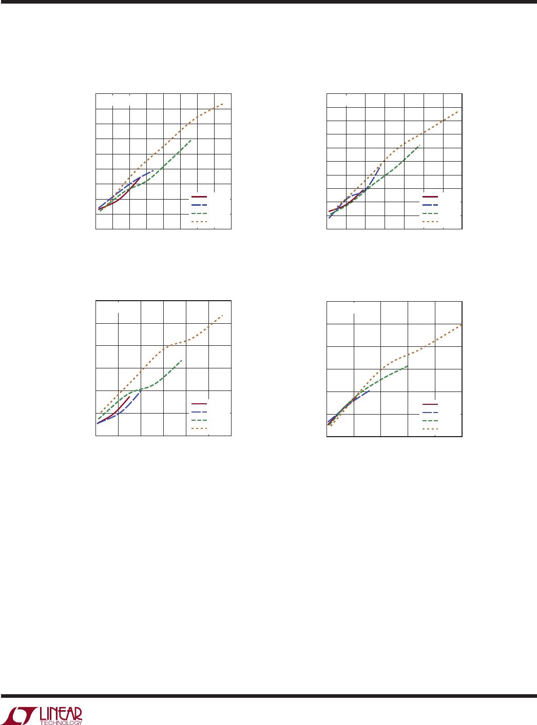
Junction Temperature Rise
vs Load Current
Junction Temperature Rise
vs Load Current
Junction Temperature Rise
vs Load Current
Junction Temperature Rise
vs Load Current
V
OUT
LOAD CURRENT (mA)
TEMPERATURE RISE (°C)
9
8
4
6
0
5
7
2
3
1
8057 G25
0 100 400200 35030025015050
3.3V
IN
5V
IN
12V
IN
24V
IN
V
OUT
= 3.3V
V
OUT
LOAD CURRENT (mA)
TEMPERATURE RISE (°C)
10
9
8
4
6
0
5
7
2
3
1
8057 G26
0 100 350200 30025015050
3.3V
IN
5V
IN
12V
IN
24V
IN
V
OUT
= 5V
V
OUT
LOAD CURRENT (mA)
TEMPERATURE RISE (°C)
12
10
8
4
6
0
2
0 100 300200 25015050
3.3V
IN
5V
IN
12V
IN
24V
IN
V
OUT
= 8V
V
OUT
LOAD CURRENT (mA)
TEMPERATURE RISE (°C)
12
10
8
4
6
0
2
8057 G28
0 100 25020015050
3.3V
IN
5V
IN
12V
IN
24V
IN
V
OUT
= 12V
LTM8057
8
8057f
For more information www.linear.com/LTM8057
PIN FUNCTIONS
V
OUT
(Bank 1): V
OUT
and V
OUT
comprise the isolated
output of the LTM8057 flyback stage. Apply an external
capacitor between V
OUT
and V
OUT
. Do not allow V
OUT
to
exceed V
OUT
.
V
OUT
(Bank 2): V
OUT
is the return for both V
OUT1
and
V
OUT2
. V
OUT1
and V
OUT
comprise the isolated output of
the LTM8057. In most applications, the bulk of the heat
flow out of the LTM8057 is through the GND and V
OUT
pads, so the printed circuit design has a large impact on
the thermal performance of the part. See the PCB Layout
and Thermal Considerations sections for more details.
Apply an external capacitor between V
OUT
and V
OUT
.
GND (Bank 4): This is the primary side local ground of the
LTM8057 primary. In most applications, the bulk of the heat
flow out of the LTM8057 is through the GND and V
OUT
pads, so the printed circuit design has a large impact on
the thermal performance of the part. See the PCB Layout
and Thermal Considerations sections for more details.
V
IN
(Bank 5): V
IN
supplies current to the LTM8057’s inter-
nal regulator and to the integrated power switch. These
pins must be locally bypassed with an external, low ESR
capacitor.
RUN (Pin F3):
A resistive divider connected to V
IN
and this
pin programs the minimum voltage at which the LTM8057
will operate. Below 1.24V, the LTM8057 does not deliver
power to the secondary. Above 1.24V, power will be de
-
livered to the secondary and 10µA will be fed into the SS
pin. When RUN is less than 1.24V, the pin draws 2.5µA,
allowing for a programmable hysteresis. Do not allow a
negative voltage (relative to GND) on this pin. T
ie this pin
to V
IN
if it is not used.
ADJ (Pins G7): Apply a resistor from this pin to GND to
set the output voltage V
OUT1
relative to V
OUT
, using the
recommended value given in Table 1. If Table 1 does not
list the desired V
OUT
value, the equation:
R
ADJ
= 28.4 V
OUT1
0.879
( )
k
may be used to approximate the value. To the seasoned
designer, this exponential equation may seem unusual. The
equation is exponential due to nonlinear current sources
that are used to temperature compensate the regulation.
BIAS (Pin H5): This pin supplies the power necessary to
operate the LTM8057. It must be locally bypassed with a
low ESR capacitor of at least 4.7μF. Do not allow this pin
voltage to rise above V
IN
.
SS (Pin H6): Place a soft-start capacitor here to limit inrush
current and the output voltage ramp rate. Do not allow a
negative voltage (relative to GND) on this pin.
PACKAGE ROW AND COLUMN LABELING MAY VARY
AMONG µModule PRODUCTS. REVIEW EACH PACKAGE
LAYOUT CAREFULLY.
LTM8057
9
8057f
For more information www.linear.com/LTM8057
BLOCK DIAGRAM
OPERATION
The LTM8057 is a stand-alone isolated flyback switching
DC/DC power supply that can deliver up to 440mA of output
current. This module provides a regulated output voltage
programmable via one external resistor from 2.5V to 12V.
The input voltage range of the LTM8057 is 3.1V to 31V.
Given that the LTM8057 is a flyback converter, the output
current depends upon the input and output voltages, so
make sure that the input voltage is high enough to support
the desired output voltage and load current. The Typical
Performance Characteristics section gives several graphs
of the maximum load versus V
IN
for several output voltages.
A simplified block diagram is given. The LTM8057 contains
a current mode controller, power switching element, power
transformer, power Schottky diode and a modest amount
of input and output capacitance.
The LTM8057 has a galvanic primary to secondary isola
-
tion rating of 2kV AC. This is verified by applying 3kV DC
between the primary and secondary for 1 second. Note that
the 2kV AC isolation is verified by a 3kV DC test. The peak
voltage of a 2kV AC waveform is 2.83kV DC, so 3kV DC is
applied. For details please refer to the Isolation, Working
Voltage and Safely Compliance section. The LTM8057 is
a UL 60950 recognized component.
An internal regulator provides power to the control cir
-
cuitry. The bias regulator normally draws power from the
V
IN
pin, but if the BIAS pin is connected to an external
voltage higher than 3.1V, bias power will be drawn from
the external source, improving efficiency. V
BIAS
must not
exceed V
IN
. The RUN pin is used to turn on or off the
LTM8057, disconnecting the output and reducing the input
current to 1μA or less.
The LTM8057 is a variable frequency device. For a fixed
input and output voltage, the frequency increases as the
load increases. For light loads, the current through the
internal transformer may be discontinuous.
V
IN
RUN
ADJ
*DO NOT ALLOW BIAS VOLTAGE TO BE ABOVE V
IN
GND
0.1µF
F
V
OUT
CURRENT
MODE
CONTROLLER
V
OUT
SS
BIAS*
8057 BD

LTM8057IY#PBF

Mfr. #:
Manufacturer:
Analog Devices / Linear Technology
Description:
Switching Voltage Regulators 2kVAC Isolated, 1.5W Module DC/DC Converter
Lifecycle:
New from this manufacturer.
Delivery:
DHL FedEx Ups TNT EMS
Payment:
T/T Paypal Visa MoneyGram Western Union