LTC1727/LTC1728
7
17278fd
For more information www.linear.com/LTC1727
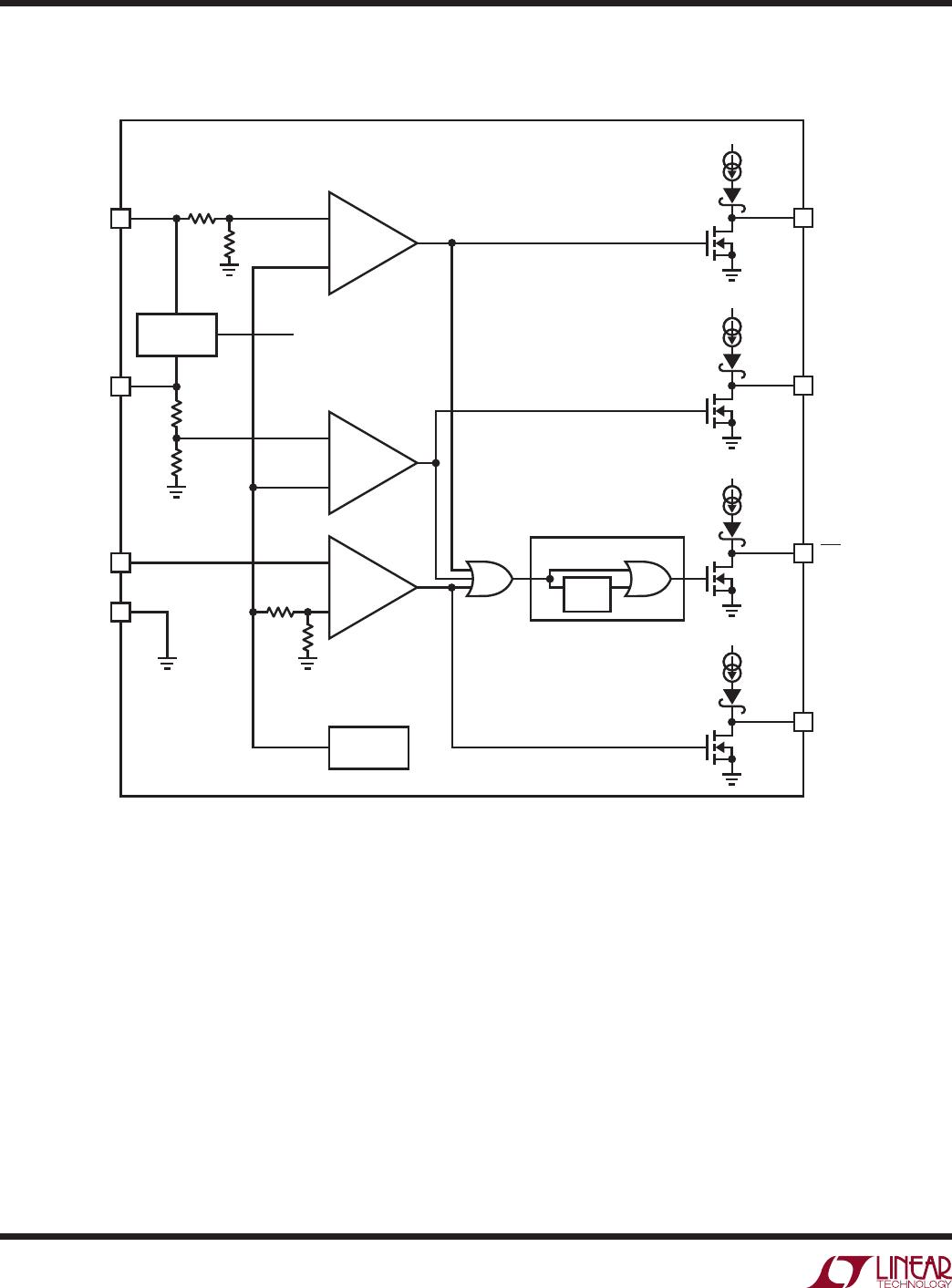
PIN FUNCTIONS
V
CC3
(Pin 1/Pin 5): 3.3V Sense Input and Power Supply
Pin. (3V Sense Input and Power Supply Pin for LTC1728-
1.8.) This pin provides power to the part when the voltage
on V
CC3
is greater than the voltage on V
CC5
/V
CC25
/V
CC18
.
Bypass to ground with a ≥0.1µF ceramic capacito
r
.
V
CC5
(Pin 2/Pin 4): 5V Sense Input and Power Supply Pin.
This pin is used on the LTC1727-5/LTC1728-5 to provide
power to the part when the voltage on V
CC5
is greater
than the voltage on V
CC3
. Bypass to ground with a ≥0.1µF
ceramic capacito
r
.
V
CC25
(Pin 2/Pin 4): 2.5V Sense Input and Power Supply
Pin. This pin is used on the LTC1727-2.5/LTC1728-2.5 to
provide power to the part when the voltage on V
CC25
is
greater than the voltage on V
CC3
. Bypass to ground with
a ≥0.1µF ceramic capacito
r
.
V
CC18
(Pin 2/Pin 4): 1.8V Sense Input and Power Supply
Pin. This pin is used on the LTC1728-1.8/LTC1728-3.3 to
provide power to the part when the voltage on V
CC18
is
greater than the voltage on V
CC3
. Bypass to ground with
a ≥0.1µF ceramic capacito
r
.
V
CCA
(Pin 3/Pin 3): 1V Sense, High Impedance Input. If un-
used, it can be tied to either V
CC3
or V
CC5
/V
CC25
/V
CC18
.
GND (Pin 4/Pin 2): Ground.
COMPA (Pin 5): V
CCA
Comparator Output for the LTC1727.
Active high, open-drain logic output with weak pull-up to
V
CC3
. Asserted when V
CCA
is above V
RTA
. Deasserted when
V
CCA
is below V
RTA
or if both the V
CC3
and V
CC5
supply
pins are too low to power the internal bandgap reference
(typically <2.0V). Can be pulled greater than V
CC3
using
an external pull-up.
RST (Pin 6/Pin 1): Reset Logic Output. Active low, open-
drain logic output with weak pull-up to V
CC3
. Can be pulled
up greater than V
CC3
when interfacing to 5V logic. Asserted
when one or all of the supplies are below trip thresholds
and held for 200ms after all supplies become valid.
COMP5 (Pin 7): V
CC5
Comparator Output for the
LTC1727-5. Active high, open-drain logic output with weak
pull-up to V
CC3
. Asserted when V
CC5
is above V
RT5
. Can
be pulled greater than V
CC3
using an external pull-up.
COMP25 (Pin 7): V
CC25
Comparator Output for the
LTC1727-2.5. Active high, open-drain logic output with
weak pull-up to V
CC3
. Asserted when V
CC25
is above
V
RT25
. Can be pulled greater than V
CC3
using an external
pull-up.
COMP3 (Pin 8): V
CC3
Comparator Output for the LTC1727.
Active high, open-drain logic output with weak pull-up to
V
CC3
. Asserted when V
CC3
is above V
RT3
. Can be pulled
greater than V
CC3
using an external pull-up.
(LTC1727/LTC1728)