IRF6811STRPBF

IRF6811SPbF
4 www.irf.com
Fig 5. Typical Output Characteristics
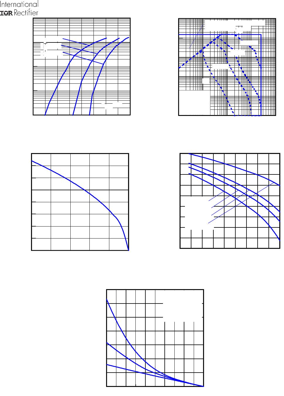
Fig 4. Typical Output Characteristics
Fig 6. Typical Transfer Characteristics
Fig 7. Normalized On-Resistance vs. Temperature
Fig 8. Typical Capacitance vs.Drain-to-Source Voltage
Fig 9. Typical On-Resistance vs.
Drain Current and Gate Voltage
0.1 1 10 100 1000
V
DS
, Drain-to-Source Voltage (V)
0.1
1
10
100
1000
I
D
,
D
r
a
i
n
-
t
o
-
S
o
u
r
c
e
C
u
r
r
e
n
t
(
A
)
VGS
TOP 10V
5.0V
4.5V
3.5V
3.3V
3.0V
2.8V
BOTTOM 2.5V
60µs PULSE WIDTH
Tj = 25°C
2.5V
0.1 1 10 100 1000
V
DS
, Drain-to-Source Voltage (V)
1
10
100
1000
I
D
,
D
r
a
i
n
-
t
o
-
S
o
u
r
c
e
C
u
r
r
e
n
t
(
A
)
2.5V
60µs PULSE WIDTH
Tj = 150°C
VGS
TOP 10V
5.0V
4.5V
3.5V
3.3V
3.0V
2.8V
BOTTOM 2.5V
1 2 3 4
V
GS
, Gate-to-Source Voltage (V)
0.1
1
10
100
1000
I
D
,
D
r
a
i
n
-
t
o
-
S
o
u
r
c
e
C
u
r
r
e
n
t
(
A
)
T
J
= 150°C
T
J
= 25°C
T
J
= -40°C
V
DS
= 15V
60µs PULSE WIDTH
-60 -40 -20 0 20 40 60 80 100 120 140 160
T
J
, Junction Temperature (°C)
0.5
1.0
1.5
2.0
T
y
p
i
c
a
l
R
D
S
(
o
n
)
(
N
o
r
m
a
l
i
z
e
d
)
I
D
= 19A
V
GS
= 10V
V
GS
= 4.5V
1 10 100
V
DS
, Drain-to-Source Voltage (V)
10
100
1000
10000
100000
C
,
C
a
p
a
c
i
t
a
n
c
e
(
p
F
)
V
GS
= 0V, f = 1 MHZ
C
iss
= C
gs
+ C
gd
, C
ds
SHORTED
C
rss
= C
gd
C
oss
= C
ds
+ C
gd
C
oss
C
rss
C
iss
0 20 40 60 80 100 120 140 160
I
D
, Drain Current (A)
0
5
10
15
20
25
30
35
40
45
T
y
p
i
c
a
l
R
D
S
(
o
n
)
(
m
)
T
J
= 25°C
Vgs = 3.5V
Vgs = 4.0V
Vgs = 4.5V
Vgs = 5.0V
Vgs = 10V
IRF6811SPbF
www.irf.com 5
Fig 13. Typical Threshold Voltage vs. Junction
Temperature
Fig 12. Maximum Drain Current vs. Case Temperature
Fig 10. Typical Source-Drain Diode Forward Voltage Fig11. Maximum Safe Operating Area
Fig 14. Maximum Avalanche Energy vs. Drain Current
0.2 0.3 0.4 0.5 0.6 0.7 0.8 0.9 1.0
V
SD
, Source-to-Drain Voltage (V)
0
1
10
100
1000
I
S
D
,
R
e
v
e
r
s
e
D
r
a
i
n
C
u
r
r
e
n
t
(
A
)
T
J
= 150°C
T
J
= 25°C
T
J
= -40°C
V
GS
= 0V
25 50 75 100 125 150
T
C
, Case Temperature (°C)
0
10
20
30
40
50
60
70
80
I
D
,
D
r
a
i
n
C
u
r
r
e
n
t
(
A
)
-75 -50 -25 0 25 50 75 100 125 150
T
J
, Temperature ( °C )
0.6
0.8
1.0
1.2
1.4
1.6
1.8
2.0
2.2
2.4
T
y
p
i
c
a
l
V
G
S
(
t
h
)
G
a
t
e
t
h
r
e
s
h
o
l
d
V
o
l
t
a
g
e
(
V
)
I
D
= 25µA
I
D
= 250µA
I
D
= 1.0mA
I
D
= 1.0A
25 50 75 100 125 150
Starting T
J
, Junction Temperature (°C)
0
20
40
60
80
100
120
140
E
A
S
,
S
i
n
g
l
e
P
u
l
s
e
A
v
a
l
a
n
c
h
e
E
n
e
r
g
y
(
m
J
)
I
D
TOP 1.4A
2.2A
BOTTOM 15A
0.01 0.10 1.00 10.00 100.00
V
DS
, Drain-to-Source Voltage (V)
0.01
0.1
1
10
100
1000
I
D
,
D
r
a
i
n
-
t
o
-
S
o
u
r
c
e
C
u
r
r
e
n
t
(
A
)
OPERATION IN THIS AREA
LIMITED BY R
DS
(on)
T
A
= 25°C
T
J
= 150°C
Single Pulse
100µsec
1msec
10msec
DC
IRF6811SPbF
6 www.irf.com
Fig 15a. Gate Charge Test Circuit
Fig 15b. Gate Charge Waveform
Vds
Vgs
Id
Vgs(th)
Qgs1
Qgs2 Qgd Qgodr
Fig 16b. Unclamped Inductive Waveforms
t
p
V
(BR)DSS
I
AS
Fig 16a. Unclamped Inductive Test Circuit
Fig 17b. Switching Time Waveforms
V
GS
V
DS
90%
10%
t
d(on)
t
d(off)
t
r
t
f
Fig 17a. Switching Time Test Circuit
R
G
I
AS
0.01
t
p
D.U.T
L
V
DS
+
-
V
DD
DRIVER
A
15V
20V
V
GS
1K
VCC
DUT
0
L
V
DS
Pulse Width ≤ 1 µs
Duty Factor ≤ 0.1 %
R
D
V
GS
R
G
D.U.T.
10V
+
-
V
DD
V
GS

IRF6811STRPBF

Mfr. #:
Manufacturer:
Infineon / IR
Description:
MOSFET 25V 1 N-CH HEXFET 3.7mOhms 11nC
Lifecycle:
New from this manufacturer.
Delivery:
DHL FedEx Ups TNT EMS
Payment:
T/T Paypal Visa MoneyGram Western Union

Products related to this Datasheet