MAX1649/MAX1651
5V/3.3V or Adjustable, High-Efficiency,
Low-Dropout, Step-Down DC-DC Controllers
10 ______________________________________________________________________________________
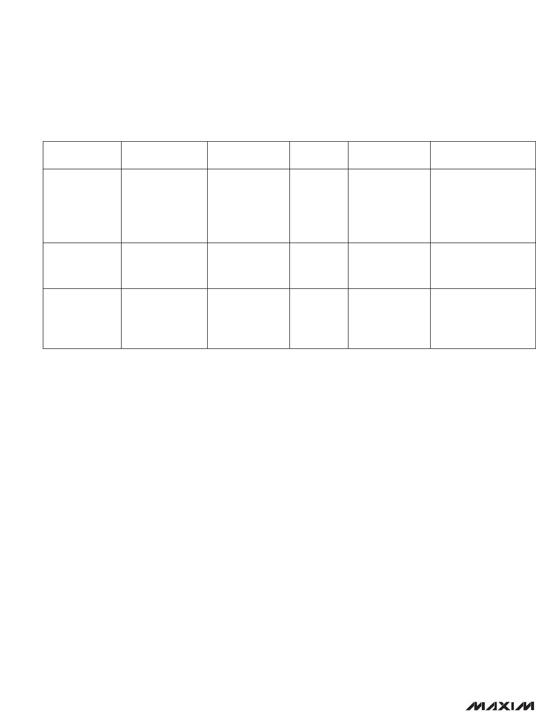
Table 1. Component Selection Guide
The peak current of Figure 1 is 2.35A for a 1.5A output.
The inductor used in this circuit is specified to drop by
10% at 2.2A (worst case); a curve provided by the
manufacturer shows that the inductance typically drops
by 20% at 2.7A. Using a slightly underrated inductor
can sometimes reduce size and cost, with only a minor
impact on efficiency.
Table 1 lists inductor types and suppliers for various
applications. The efficiencies of the listed surface-
mount inductors are nearly equivalent to those of the
larger size through-hole versions.
Diode Selection
The MAX1649/MAX1651’s high switching frequency
demands a high-speed rectifier. Schottky diodes, such
as the 1N5817 through 1N5823 (and their surface-
mount equivalents), are recommended. Choose a
diode with an average current rating equal to or greater
than I
LIM
(max) and a voltage rating higher than
V+(max).
External Switching Transistor
The MAX1649/MAX1651 drive P-channel enhancement-
mode MOSFET transistors only. The choice of power
transistor is primarily dictated by the input voltage and
the peak current. The transistor’s on-resistance, gate-
source threshold, and gate charge must also be appro-
priately chosen. The drain-to-source and gate-to-
source breakdown voltage ratings must be greater than
V+. The total gate-charge specification is normally not
critical, but values should be less than 100nC for best
efficiency. The MOSFET should be capable of handling
the peak current and, for maximum efficiency, have a
very low on-resistance at that current. Also, the on-
resistance must be low for the minimum available V
GS
,
which equals V+(min). Select a transistor with an on-
resistance between 50% and 100% of the current-
sense resistor. The Si9430 transistor chosen for the
Typical Operating Circuit has a drain-to-source rating
of -20V and a typical on-resistance of 0.070Ω at 2A with
V
GS
= -4.5V. Tables 1 and 2 list suppliers of switching
transistors suitable for use with these devices.
Capacitor Selection
Output Filter Capacitor
The primary criterion for selecting the output filter
capacitor is low equivalent series resistance (ESR),
rather than high capacitance. An electrolytic capacitor
with low enough ESR will automatically have high
enough capacitance. The product of the inductor-cur-
rent variation and the output filter capacitor’s ESR
determines the amplitude of the high-frequency ripple
seen on the output voltage. When a 330µF, 10V
Sprague surface-mount capacitor (595D series) with
ESR = 0.15Ω is used, 40mV of output ripple is typically
observed when stepping down from 10V to 5V at 1A.
The output filter capacitor's ESR also affects efficiency.
Again, low-ESR capacitors perform best. Table 1 lists
some suppliers of low-ESR capacitors.
PRODUCTION
METHOD
INDUCTORS CAPACITORS DIODES
CURRENT-SENSE
RESISTORS
MOSFETS
Surface Mount
AVX
TPS series
Sprague
595D series
Motorola
MBRS340T3
Nihon
NSQ series
Dale
WSL Series
IRC
LRC series
Miniature
Through-Hole
Sumida
RCH875-470M (1.3A)
Sanyo
OS-CON series
low-ESR organic
semiconductor
IRC
OAR series
Motorola
Low-Cost
Through-Hole
Coilcraft
PCH-45-473 (3.4A)
Motorola
1N5817 to
1N5823
Motorola
TMOS power MOSFETs
Sumida
CDRH125-470 (1.8A)
CDRH125-220 (2.2A)
Coilcraft
DO3316-473 (1.6A)
DO3340-473 (3.8A)
Siliconix
Little Foot series
Motorola
medium-power
surface-mount products
Nichicon
PL series
low-ESR electrolytics
United Chemi-Con
LXF series
Input Bypass Capacitor
The input bypass capacitor reduces peak currents
drawn from the voltage source, and also reduces the
amount of noise at the voltage source caused by the
switching action of the MAX1649/MAX1651. The input
voltage source impedance determines the size of the
capacitor required at the V+ input. As with the output fil-
ter capacitor, a low-ESR capacitor is recommended.
Bypass the IC separately with a 0.1µF ceramic capac-
itor placed close to the V+ and GND pins.
Reference Capacitor
Bypass REF with a 0.1µF or larger capacitor.
MAX1649/MAX1651
5V/3.3V or Adjustable, High-Efficiency,
Low-Dropout, Step-Down DC-DC Controllers
______________________________________________________________________________________ 11
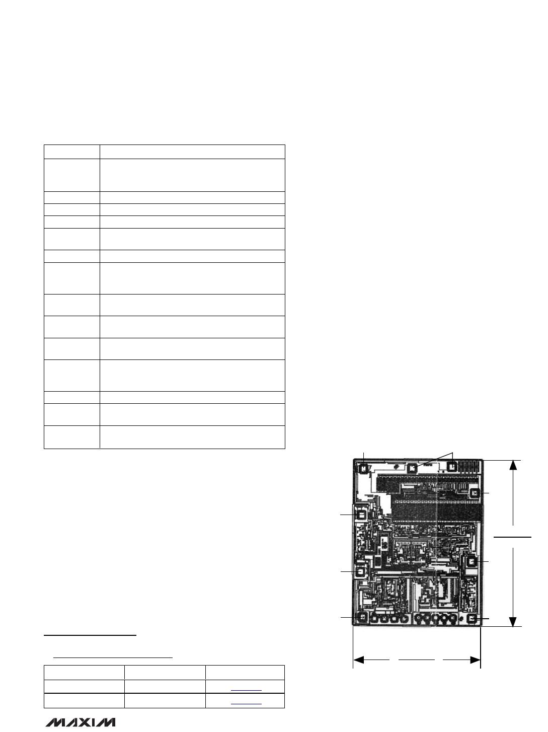
___________________Chip Topography
TRANSISTOR COUNT: 428
SUBSTRATE CONNECTED TO V+
0.106"
(2.692mm)
0.081"
(2.057mm)
OUT
GND
CS
EXT
V+
FB
SHDN
REF
Table 2. Component Suppliers
COMPANY PHONE FAX
(207) 282-5111
AVX USA or (207) 283-1941
(800) 282-4975
Coiltronics USA (516) 241-7876 (516) 241-9339
Coilcraft USA (708) 639-6400 (708) 639-1469
Dale USA (402) 564-3131 (402) 563-1841
International
USA (310) 322-3331 (310) 322-3332
Rectifier
IRC USA (512) 992-7900 (512) 992-3377
(602) 244-3576
Motorola USA or (602) 244-4015
(602) 244-5303
Nichicon
USA (708) 843-7500 (708) 843-2798
Japan 81-7-5231-8461 81-7-5256-4158
Nihon
USA (805) 867-2555 (805) 867-2556
Japan 81-3-3494-7411 81-3-3494-7414
Sanyo
USA (619) 661-6835 (619) 661-1055
Japan 81-7-2070-6306 81-7-2070-1174
(408) 988-8000
Siliconix USA or (408) 970-3950
(800) 554-5565
Sprague USA (603) 224-1961 (603) 224-1430
Sumida
USA (708) 956-0666 (708) 956-0702
Japan 81-3-3607-5111 81-3-3607-5144
United
USA (714) 255-9500 (714) 255-9400
Chemi-Con
Layout Considerations
Proper PC board layout is essential because of high
current levels and fast switching waveforms that radi-
ate noise. Minimize ground noise by connecting the
anode of the rectifier, the input bypass capacitor
ground lead, and the output filter capacitor ground
lead to a single point (“star” ground configuration). A
ground plane is recommended. Also minimize lead
lengths to reduce stray capacitance, trace resistance,
and radiated noise. In particular, the traces connected
to FB (if an external resistor divider is used) and EXT
must be short. Place the 0.1µF ceramic bypass capac-
itor as close as possible to the V+ and GND pins.
MAX1649/MAX1651 vs. MAX649/MAX651
The MAX1649 and MAX1651 are pin compatible with
the MAX649 and MAX651, but have been optimized for
improved dropout performance and efficiency—partic-
ularly with low input voltages. The MAX1649/MAX1651
feature increased maximum switch duty cycle (96.5%)
and reduced current-limit sense voltage (110mV).
Their predecessors, the MAX649/MAX651, use a high-
er two-step (210mV/110mV) current-limit sense voltage
to provide tighter current-sense accuracy and reduced
inductor peak current at light loads.
Package Information
For the latest package outline information and land patterns, go
to www.maxim-ic.com/packages
.
PACKAGE TYPE PACKAGE CODE DOCUMENT NO.
8 PDIP P8-2 21-0041
8 SO S8-4 21-0043
Maxim cannot assume responsibility for use of any circuitry other than circuitry entirely embodied in a Maxim product. No circuit patent licenses are
implied. Maxim reserves the right to change the circuitry and specifications without notice at any time.
12 __________________Maxim Integrated Products, 120 San Gabriel Drive, Sunnyvale, CA 94086 (408) 737-7600
© 2009 Maxim Integrated Products Maxim is a registered trademark of Maxim Integrated Products, Inc.
MAX1649/MAX1651
5V/3.3V or Adjustable, High-Efficiency,
Low-Dropout, Step-Down DC-DC Controllers
Revision History
REVISION
NUMBER
REVISION
DATE
DESCRIPTION
PAGES
CHANGED
3 3/09 Corrected Output Voltage conditions and Figure 1 title 2, 6

MAX1649EPA

Mfr. #:
Manufacturer:
Maxim Integrated
Description:
LDO Voltage Controllers 5V/3.3V or Adjustable, High-Efficiency, Low-Dropout, Step-Down DC-DC Controller
Lifecycle:
New from this manufacturer.
Delivery:
DHL FedEx Ups TNT EMS
Payment:
T/T Paypal Visa MoneyGram Western Union