2001-2012 Microchip Technology Inc. DS21468B-page 5
TC7662A
3.0 DETAILED DESCRIPTION
The TC7662A is a capacitive charge pump (sometimes
called a switched-capacitor circuit), where four
MOSFET switches control the charge and discharge of
a capacitor.
The functional block diagram shows how the switching
action works. SW1 and SW2 are turned on simulta-
neously, charging C
P
to the supply voltage, V
DD
. This
assumes that the ON resistance of the MOSFETs in
series with the capacitor produce a charging time
(3 time constants) less than the ON time provided by
the oscillator frequency, as shown:
3 (R
DS(ON)
C
P
) <C
P
/(0.5 f
OSC
).
In the next cycle, SW1 and SW2 are turned OFF and,
after a very short interval with all switches OFF
(preventing large currents from occurring due to cross
conduction), SW3 and SW4 are turned ON. The charge
in C
P
is then transferred to C
R
, but with the polarity
inverted. In this way, a negative voltage is derived.
An oscillator supplies pulses to a flip-flop that is fed to
a set of level shifters. These level shifters then drive
each set of switches at one-half the oscillator
frequency.
The oscillator has a pin that controls the frequency
of oscillation. Pin 7 can have a capacitor added that
is connected to ground. This will lower the frequency
of the oscillator by adding capacitance to the
internal timing capacitor of the TC7662A. (See Typical
Characteristics – Oscillator Frequency vs. C
OSC
.)
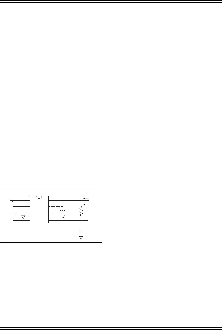
FIGURE 3-1: TC7662A TEST CIRCUIT
3.1 Theoretical Power Efficiency
Considerations
In theory, a voltage converter can approach 100%
efficiency if certain conditions are met:
1. The drive circuitry consumes minimal power.
2. The output switches have extremely low ON
resistance and virtually no offset.
3. The impedances of the pump and reservoir
capacitors are negligible at the pump frequency.
The TC7662A approaches these conditions for
negative voltage conversion if large values of C
P
and
C
R
are used.
Note: Energy is lost only in the transfer of charge
between capacitors if a change in voltage
occurs.
The energy lost is defined by:
E = 1/2 C
P
(V
1
2
– V
2
2
)
V
1
and V
2
are the voltages on C
P
during the pump and
transfer cycles. If the impedances of C
P
and C
R
are
relatively high at the pump frequency (refer to Figure 3-
1), compared to the value of R
L
, there will be a
substantial difference in voltages V
1
and V
2
. Therefore,
it is desirable not only to make C
R
as large as possible
to eliminate output voltage ripple, but also to employ a
correspondingly large value for C
P
in order to achieve
maximum efficiency of operation.
3.2 Dos and Don'ts
• Do not exceed maximum supply voltages.
• Do not short circuit the output to V
+
supply for
voltages above 5.5V for extended periods;
however, transient conditions including start-up
are okay.
• When using polarized capacitors in the inverting
mode, the + terminal of C
P
must be connected to
pin 2 of the TC7662A and the + terminal of C
R
must be connected to GND (pin 3).
• If the voltage supply driving the TC7662A has a
large source impedance (25-30 ohms), then a
2.2F capacitor from pin 8 to ground may be
required to limit the rate of rise of the input voltage
to less than 2V/sec.
TC7662A
1
2
3
4
8
7
5
+
10μF
10μF
V
DD
(+5V)
NC
NC
6
+
C
P
C
R
V
OUT
(-5V)
C
OSC
R
L
I
S
I
L