2001-2012 Microchip Technology Inc. DS21468B-page 7
TC7662A
4.2 Output Ripple
ESR also affects the ripple voltage seen at the output.
The total ripple is determined by 2 voltages, A and B,
as shown in Figure 4-2. Segment A is the voltage drop
across the ESR of C
R
at the instant it goes from being
charged by C
P
(current flowing into C
R
) to being dis-
charged through the load (current flowing out of C
R
).
The magnitude of this current change is 2 x I
OUT
, hence
the total drop is 2 x I
OUT
x ESR
CR
volts. Segment B is
the voltage change across C
R
during time t
2
, the half of
the cycle when C
R
supplies current to the load. The
drop at B is I
OUT
x t
2
/C
R
volts. The peak-to-peak ripple
voltage is the sum of these voltage drops:
FIGURE 4-2: OUTPUT RIPPLE
4.3 Paralleling Devices
Any number of TC7662A voltage converters may be
paralleled to reduce output resistance (Figure 4-3).
The reservoir capacitor, C
R
, serves all devices, while
each device requires its own pump capacitor, C
P
. The
resultant output resistance would be approximately:
4.4 Cascading Devices
The TC7662A may be cascaded as shown (Figure 4-4)
to produce larger negative multiplication of the initial
supply voltage. However, due to the finite efficiency of
each device, the practical limit is 10 devices for light
loads. The output voltage is defined by:
V
OUT
= – n (V
IN
)
where n is an integer representing the number of
devices cascaded. The resulting output resistance
would be approximately the weighted sum of the
individual TC7662A R
OUT
values.
FIGURE 4-3: PARALLELING DEVICES LOWERS OUTPUT IMPEDANCE
FIGURE 4-4: INCREASED OUTPUT VOLTAGE BY CASCADING DEVICES
1
2 x f
PUMP
x C
R
V
RIPPLE
( + 2 x ESR
CR
x I
OUT
)
t
2
t
1
B
A
V
0
-(V
DD
)
R
OUT
=
R
OUT
(of TC7662A)
n (number of devices)
1
2
3
4
8
7
6
5
TC7662A
V
DD
1
2
3
4
8
7
6
5
TC7662A
R
L
C
2
C
1
"n"
"1"
+
C
1
TC7662A
DS21468B-page 8 2001-2012 Microchip Technology Inc.
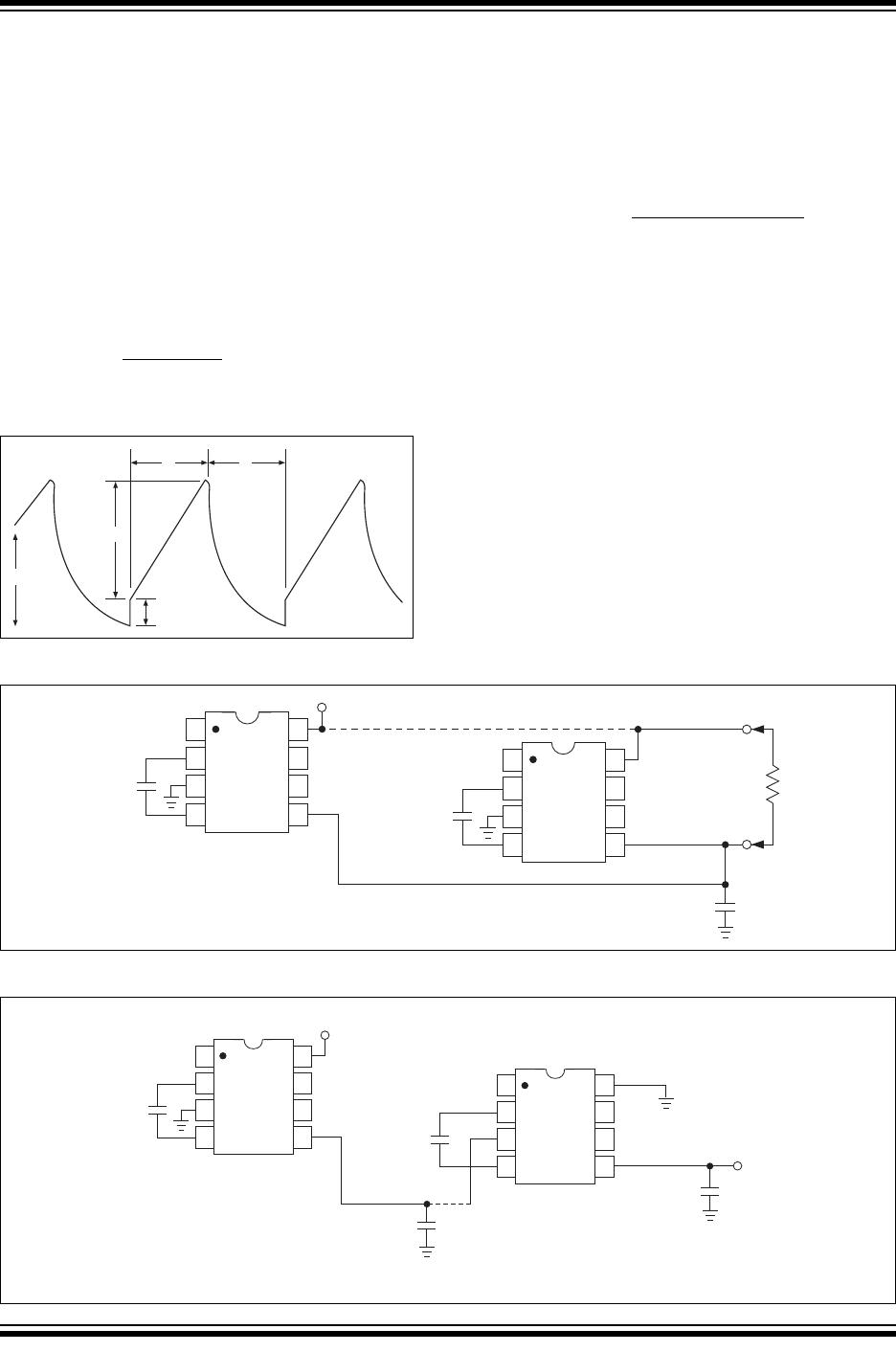
4.5 Changing the TC7662A Oscillator
Frequency
It is possible to increase the conversion efficiency of
the TC7662A at low load levels by lowering the
oscillator frequency. This reduces the switching losses,
and is shown in Figure 4-5. However, lowering the
oscillator frequency will cause an undesirable increase
in the impedance of the pump (C
P
) and reservoir (C
R
)
capacitors; this is overcome by increasing the values of
C
P
and C
R
by the same factor that the frequency has
been reduced. For example, the addition of a 100pF
capacitor between pin 7 (OSC) and V
DD
will lower the
oscillator frequency to 2kHz from its nominal frequency
of 12kHz (multiple of 6), and thereby necessitate a
corresponding increase in the value of C
P
and C
R
(from
10F to 68F).
FIGURE 4-5: LOWERING OSCILLATOR
FREQUENCY
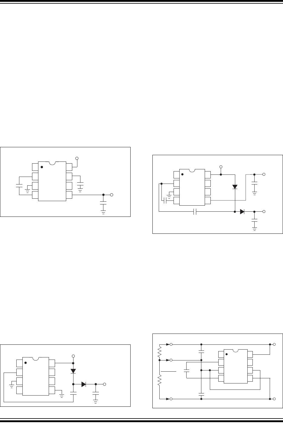
4.6 Positive Voltage Doubling
The TC7662A may be employed to achieve positive
voltage doubling using the circuit shown in Figure 4-6.
In this application, the pump inverter switches of the
TC7662A are used to charge C
P
to a voltage level of
V
DD
– V
F
(where V
DD
is the supply voltage and V
F
is
the forward voltage on C
P
plus the supply voltage (V
DD
)
applied through diode D
2
to capacitor C
R
). The voltage
thus created on C
R
becomes (2 V
DD
) – (2 V
F
), or twice
the supply voltage minus the combined forward voltage
drops of diodes D
1
and D
2
.
The source impedance of the output (V
OUT
) will depend
on the output current, but for V
DD
= 5V and an output
current of 10 mA, it will be approximately 60.
FIGURE 4-6: POSITIVE VOLTAGE
MULTIPLIER
4.7 Combined Negative Voltage
Conversion and Positive Supply
Multiplication
Figure 4-7 combines the functions shown in Figure 4-1
and Figure 4-6 to provide negative voltage conversion
and positive voltage doubling simultaneously. This
approach would be, for example, suitable for generat-
ing +9V and -5V from an existing +5V supply. In this
instance, capacitors C
1
and C
3
perform the pump and
reservoir functions, respectively, for the generation of
the negative voltage, while capacitors C
2
and C
4
are
pump and reservoir, respectively, for the doubled
positive voltage. There is a penalty in this configuration
which combines both functions, however, in that the
source impedances of the generated supplies will be
somewhat higher due to the finite impedance of the
common charge pump driver at pin 2 of the device.
FIGURE 4-7: COMBINED NEGATIVE
CONVERTER AND
POSITIVE DOUBLER
4.8 Voltage Splitting
The same bidirectional characteristics can be used to
split a higher supply in half, as shown in Figure 4-8.
The combined load will be evenly shared between the
two sides. Because the switches share the load in
parallel, the output impedance is much lower than in
the standard circuits, and higher currents can be drawn
from the device. By using this circuit, and then the
circuit of Figure 4-4, +15V can be converted (via +7.5V
and -7.5V) to a nominal -15V, though with rather high
series resistance (~250).
FIGURE 4-8: SPLITTING A SUPPLY IN
HALF
1
2
3
4
8
7
6
5
+
V
OUT
C
OSC
+
TC7662A
10μF
10μF
V
DD
1
2
3
4
8
7
6
5
V
OUT
=
(2 V
DD
) – (2 V
F
)
+
C
R
D
1
D
2
+
C
P
TC7662A
V
DD
1
2
3
4
8
7
6
5
+
V
DD
V
OUT
=
(2 V
DD
) – (2 V
F
)
C
1
D
1
+
+
C
3
C
4
V
OUT
=
-(V
DD
– V
F
)
C
2
TC7662A
D
2
+
+
R
L1
R
L2
V
OUT
=
V
DD
– V
2
50μF
50
μF
V
DD
V
50μF
+
1
2
8
7
TC7662A
3
4
6
5
+
2001-2012 Microchip Technology Inc. DS21468B-page 9
TC7662A
5.0 TYPICAL CHARACTERISTICS
Circuit of Figure 3-1, C
P
= C
R
= 10F, C
ESRCP
C
ESRCR
1, T
A
= 25°C unless otherwise noted.
Note: The graphs and tables provided following this note are a statistical summary based on a limited number of
samples and are provided for informational purposes only. The performance characteristics listed herein are
not tested or guaranteed. In some graphs or tables, the data presented may be outside the specified
operating range (e.g., outside specified power supply range) and therefore outside the warranted range.
700
600
500
400
300
200
100
-60 -40 -20 0 20 40 60 80 100 120 140
TEMPERATURE (°C)
SUPPLY CURRENT (μA)
V
DD
= 15V
V
DD
= 5V
0
Supply Current vs. Temperature
20
18
16
14
12
10
8
-60 -40 -20 0 20 40 60 80 100 120 140
TEMPERATURE (°C)
FREQUENCY (kHz)
6
Frequency vs. Temperature
100
LOAD CURRENT (mA)
POWER CONVERSION EFFICIENCY (%)
Power Conversion Efficiency vs. I
LOAD
16 32 48 64 80
80
60
40
20
90
70
50
30
10
8244056720
150
120
90
60
30
135
105
75
45
15
0
SUPPLY CURRENT (mA)
Efficiency
Supply
Current
110
T
A
= +25°C
165
1k
1
00
1
1
0
1
00
1
000
10
,
00
0
CAPACITANCE
(
pF
)
F
REQUENCY
(
Hz
)
1
0
Oscillator Frequenc
y
vs.
C
OSC
1
0k
T
A
T
= +2
5
°
C
160
140
120
100
80
60
40
-60 -40 -20 0 20 40 60 80 100 120 140
TEMPERATURE (°C)
OUTPUT RESISTANCE ( )
V
DD
= 15V, I
L
= 20mA
Output Resistance vs. Temperature
20
V
DD
= 5V, I
L
= 3mA
Ω
100
INPUT VOLTAGE (V)
OUTPUT RESISTANCE ( )
Output Resistance vs. Input Voltage
4 8 12 16 20
80
60
40
20
90
70
50
30
10
2 6 10 14 180
Ω
110
I
L
= 20mA
T
A
= +25°C

TC7662ACPA

Mfr. #:
Manufacturer:
Microchip Technology
Description:
Switching Voltage Regulators High Voltage
Lifecycle:
New from this manufacturer.
Delivery:
DHL FedEx Ups TNT EMS
Payment:
T/T Paypal Visa MoneyGram Western Union

Products related to this Datasheet