REV.
Information furnished by Analog Devices is believed to be accurate and
reliable. However, no responsibility is assumed by Analog Devices for its
use, nor for any infringements of patents or other rights of third parties
which may result from its use. No license is granted by implication or
otherwise under any patent or patent rights of Analog Devices.
a
AD654
One Technology Way, P.O. Box 9106, Norwood, MA 02062-9106, U.S.A.
Tel: 781/329-4700 World Wide Web Site: http://www.analog.com
Fax: © Analog Devices, Inc.,
Low Cost Monolithic
Voltage-to-Frequency Converter
FEATURES
Low Cost
Single or Dual Supply, 5 V to 36 V, ⴞ5 V to ⴞ18 V
Full-Scale Frequency Up to 500 kHz
Minimum Number of External Components Needed
Versatile Input Amplifier
Positive or Negative Voltage Modes
Negative Current Mode
High Input Impedance, Low Drift
Low Power: 2.0 mA Quiescent Current
Low Offset: 1 mV
PRODUCT DESCRIPTION
The AD654 is a monolithic V/F converter consisting of an input
amplifier, a precision oscillator system, and a high current output
stage. A single RC network is all that is required to set up any
full scale (FS) frequency up to 500 kHz and any FS input voltage
up to ±30 V. Linearity error is only 0.03% for a 250 kHz FS,
and operation is guaranteed over an 80 dB dynamic range. The
overall temperature coefficient (excluding the effects of external
components) is typically
±50 ppm/°C. The AD654 operates from
a single supply of 5 V to 36 V and consumes only 2.0 mA quies-
cent current.
The low drift (4 µV/°C typ) input amplifier allows operation
directly from small signals such as thermocouples or strain gauges
while offering a high (250 MΩ) input resistance. Unlike most
V/F converters, the AD654 provides a square-wave output, and
can drive up to 12 TTL loads, optocouplers, long cables, or
similar loads.
PRODUCT HIGHLIGHTS
1. Packaged in both an 8-lead mini-DIP and an 8-lead SOIC
package, the AD654 is a complete V/F converter requiring
only an RC timing network to set the desired full-scale fre-
quency and a selectable pull-up resistor for the open-collector
output stage. Any full scale input voltage range from 100 mV
to 10 volts (or greater, depending on +V
S
) can be accommo-
dated by proper selection of the timing resistor. The full-
scale frequency is then set by the timing capacitor from the
simple relationship, f = V/10 RC.
2. A minimum number of low cost external components are
necessary. A single RC network is all that is required to set
up any full scale frequency up to 500 kHz and any full-scale
input voltage up to ±30 V.
3. Plastic packaging allows low cost implementation of the
standard VFC applications: A/D conversion, isolated signal
transmission, F/V conversion, phase-locked loops, and tuning
switched-capacitor filters.
4. Power supply requirements are minimal; only 2.0 mA of
quiescent current is drawn from the single positive supply
from 4.5 volts to 36 volts. In this mode, positive inputs can
vary from 0 volts (ground) to (+V
S
–4) volts. Negative inputs
can easily be connected for below ground operation.
5. The versatile open-collector output stage can sink more than
10 mA with a saturation voltage less than 0.4 volts. The Logic
Common terminal can be connected to any level between
ground (or –V
S
) and 4 volts below +V
S
. This allows easy
direct interface to any logic family with either positive or
negative logic levels.
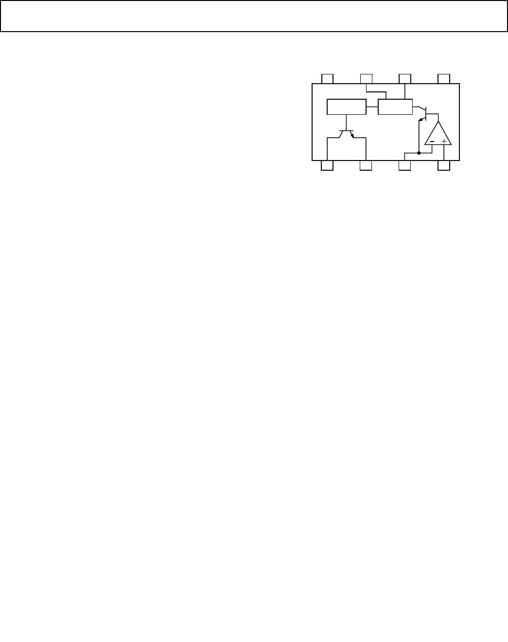
FUNCTIONAL BLOCK DIAGRAM
321
58 7 6
AD654
4
DRIVER OSC
F
OUT
LOGIC
COMMON
R
T
+V
IN
+V
S
C
T
C
T
–V
S