AD654
Rev. C | Page 3
ABSOLUTE MAXIMUM RATINGS
Parameter Rating
Total Supply Voltage +V
S
to −V
S
36 V
Maximum Input Voltage
(Pins 3, 4) to −V
S
−300 mV to +V
S
Maximum Output Current
Instantaneous 50 mA
Sustained 25 mA
Logic Common to −V
S
−500 mV to (+V
S
–4)
Storage Temperature Range −65°C to +150°C
Stresses above those listed under Absolute Maximum Ratings
may cause permanent damage to the device. This is a stress
rating only; functional operation of the device at these or any
other conditions above those indicated in the operational
section of this specification is not implied. Exposure to absolute
maximum rating conditions for extended periods may affect
device reliability.
ESD CAUTION
AD654
–4–
REV.
CIRCUIT OPERATION
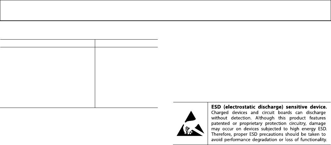
The AD654’s block diagram appears in Figure 1. A versatile
operational amplifier serves as the input stage; its purpose is to
convert and scale the input voltage signal to a drive current in the
NPN follower. Optimum performance is achieved when, at the
full-scale input voltage, a 1 mA drive current is delivered to the
current-to-frequency converter (an astable multivibrator). The
drive current provides both the bias levels and the charging current
to the externally connected timing capacitor. This “adaptive” bias
scheme allows the oscillator to provide low nonlinearity over
the entire current input range of 100 nA to 2 mA. The square
wave oscillator output goes to the output driver which provides
a floating base drive to the NPN power transistor. This floating
drive allows the logic interface to be referenced to a level other
than –V
S
.
OSC/
DRIVER
AD654
OPTIONAL
R
COMP
CR1
–V
S
(
0V TO –15V
)
R1
R2
V
IN
+V
S
(+5V TO –V
S
+30)
C
T
+V
LOGIC
R
PU
F
OUT
F
OUT
=
V
IN
(10V) (R1 + R2) C
T
Figure 1. Standard V-F Connection for Positive Input
Voltages
V/F CONNECTION FOR POSITIVE INPUT VOLTAGES
In the connection scheme of Figure 1, the input amplifier presents
a very high (250 M) impedance to the input voltage, which
is converted into the proper drive current by the scaling resistors
at Pin 3. Resistors R1 and R2 are selected to provide a 1 mA
full-scale current with enough trim range to accommodate the
AD654’s 10% FS error and the components’ tolerances. Full-
scale currents other than 1 mA can be chosen, but linearity will
be reduced; 2 mA is the maximum allowable drive. The AD654’s
positive input voltage range spans from –V
S
(ground in sink supply
operation) to four volts below the positive supply. Power sup-
ply rejection degrades as the input exceeds (+V
S
– 3.75 V) and at
(+V
S
– 3.5 V) the output frequency goes to zero.
As indicated by the scaling relationship in Figure 1, a 0.01 µF
timing capacitor will give a 10 kHz full-scale frequency, and
0.001 µF will give 100 kHz with a 1 mA drive current. Good V/F
linearity requires the use of a capacitor with low dielectric
absorption (DA), while the most stable operation over tempera-
ture calls for a component having a small tempco. Polystyrene,
polypropylene, or Teflon* capacitors are preferred for tempco and
dielectric absorption; other types will degrade linearity. The
capacitor should be wired very close to the AD654. In Figure 1,
Schottky diode CR1 (MBD101) prevents logic common from
dropping more than 500 mV below –V
S
. This diode is not
required if –V
S
is equal to logic common.
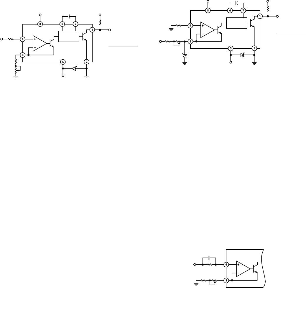
V/F CONNECTIONS FOR NEGATIVE INPUT VOLTAGE
OR CURRENT
The AD654 can accommodate a wide range of negative input
voltages with proper selection of the scaling resistor, as indicated
in Figure 2. This connection, unlike the buffered positive con-
nection, is not high impedance because the signal source must
supply the 1 mA FS drive current. However, large negative volt-
ages beyond the supply can be handled easily by modifying the
scaling resistors appropriately. If the input is a true current source,
R1 and R2 are not used. Again, diode CR1 prevents latch-up by
insuring Logic Common does not drop more than 500 mV below
–V
S
. The clamp diode (MBD101) protects the AD654 input
from “below –V
S
” inputs.
OSC/
DRIVER
AD654
OPTIONAL
R
COMP
CR1
–V
S
(0V TO –15V)
R1 R2
+V
S
(+5V TO –V
S
+30)
C
T
+V
LOGIC
R
PU
F
OUT
F
OUT
=
V
IN
(10V) (R1 + R2) C
T
V
IN
CLAMP
DIODE
Figure 2. V-F Connections for Negative Input Voltages or
Current
OFFSET CALIBRATION
In theory, two adjustments calibrate a V/F: scale and offset. In
practice, most applications find the AD654’s 1 mV max voltage
offset sufficiently low to forgo offset calibration. However, the
input amplifier’s 30 nA (typ) bias currents will generate an offset
due to the difference in dc sound resistance between the input
terminals. This offset can be substantial for large values of R
T
=
R1 + R2 and will vary as the bias currents drift over temperature.
Therefore, to maintain the AD654’s low offset, the application may
require balancing the dc source resistances at the inputs (Pins
3 and 4).
For positive inputs, this is accomplished by adding a compensation
resistor nominally equal to R
T
in series with the input as shown
in Figure 3a. This limits the offset to the product of the 30 nA
bias current and the mismatch between the source resistance R
T
and R
COMP
. A second, smaller offset arises from the inputs’ 5 nA
offset current flowing through the source resistance R
T
or R
COMP
.
For negative input voltage and current connections, the compensa-
tion resistor is added at Pin 4 as shown in Figure 3b in lieu of
grounding the pin directly. For both positive and negative inputs,
the use of R
COMP
may lead to noise coupling at Pin 4 and should
therefore be bypassed for lowest noise operation.
R1 R2
V
IN
R
COMP
AD654
(OPTIONAL)
C
Figure 3a. Bias Current Compensation—Positive Inputs
*Teflon is a trademark of E.I. Du Pont de Nemours & Co.
C
AD654
REV.
–5–
(OPTIONAL)
C
R1 R2
V
IN
R
COMP
AD654
Figure 3b. Bias Current Compensation—Negative Inputs
If the AD654’s 1 mV offset voltage must be trimmed, the trim
must be performed external to the device. Figure 3c shows an
optional connection for positive inputs in which R
OFF1
and
R
OFF2
add a variable resistance in series with R
T
. A variable
source of ±0.6 V applied to R
OFF1
then adjusts the offset ±1 mV.
Similarly, a ±0.6 V variable source is applied to R
OFF
in Fig-
ure 3d to trim offset for negative inputs. The ±0.6 V bipolar
source could simply be an AD589 reference connected as shown
in Figure 3e.
V
IN
10kV
AD654
5kV 8.25kV
R
OFF2
20V
R
OFF1
10kV
60.6V
Figure 3c. Offset Trim Positive Input (10 V FS)
V
IN
10kV
AD654
5kV8.25kV
R
OFF
5.6MV
60.6V
Figure 3d. Offset Trim Negative Input (–10 V FS)
+5V
R3
10kV
60.6V
R4
10kV
R5
100kV
+
AD589
R1
10kV
R1
10kV
R2
10kV
–5V
Figure 3e. Offset Trim Bias Network
FULL-SCALE CALIBRATION
Full-scale trim is the calibration of the circuit to produce the
desired output frequency with a full-scale input applied. In most
cases this is accomplished by adjusting the scaling resistor R
T
.
Precise calibration of the AD654 requires the use of an accurate
voltage standard set to the desired FS value and an accurate
frequency meter. A scope is handy for monitoring output wave-
shape. Verification of converter linearity requires the use of a
switchable voltage source or DAC having a linearity error below
±0.005%, and the use of long measurement intervals to mini-
mize count uncertainties. Since each AD654 is factory tested for
linearity, it is unnecessary for the end-user to perform this tedious
and time consuming test on a routine basis.
Sufficient FS calibration trim range must be provided to accom-
modate the worst-case sum of all major scaling errors. This
includes the AD654’s 10% full-scale error, the tolerance of the
fixed scaling resistor, and the tolerance of the timing capacitor.
Therefore, with a resistor tolerance of 1% and a capacitor tolerance
of 5%, the fixed part of the scaling resistor should be a maximum
of 84% of nominal, with the variable portion selected to allow
116% of the nominal.
If the input is in the form of a negative current source, the scaling
resistor is no longer required, eliminating the capability of trim-
ming FS frequency in this fashion. Since it is usually not practical
to smoothly vary the capacitance for trimming purposes, an
alternative scheme such as the one shown in Figure 4 is needed.
Designed for a FS of 1 mA, this circuit divides the input into two
AD654
R
OFF
100kV
R4
392V
R3
1kV
60.6V
*
*OPTIONAL
OFFSET TRIM
f =
I
S
(20V) C
T
I
R
–V
1mA
FS
I
S
R2
100V
R1
100V
Figure 4. Current Source FS Trim
and flowing into Pin 3; it constitutes the signal current I
T
to be
converted. The second path, through another 100 resistor R2,
carries the same nominal current. Two equal valued resistors
offer the best overall stability, and should be either 1% discrete
film units, or a pair from a common array.
Since the 1 mA FS input current is divided into two 500 µA legs
(one to ground and one to Pin 3), the total input signal current
(I
S
) is divided by a factor of two in this network. To achieve the
same conversion scale factor, C
T
must be reduced by a factor of
two. This results in a transfer unique to this hookup:
f =
I
S
(20 V ) C
T
For calibration purposes, resistors R3 and R4 are added to the
network, allowing a ±15% trim of scale factor with the values
shown. By varying R4’s value the trim range can be modified to
accommodate wider tolerance components or perhaps the cali-
bration tolerance on a current output transducer such as the
AD592 temperature sensor. Although the values of R1–R4 shown
are valid for 1 mA FS signals only, they can be scaled upward
proportionately for lower FS currents. For instance, they should
be increased by a factor of ten for a FS current of 100 µA.
In addition to the offsets generated by the input amplifier’s bias
and offset currents, an offset voltage induced parasitic current
arises from the current fork input network. These effects are
minimized by using the bias current compensation resistor R
OFF
and offset trim scheme shown in Figure 3e.
Although device warm-up drifts are small, it is good practice to
allow the devices operating environment to stabilize before trim,
C

AD654JR

Mfr. #:
Manufacturer:
Description:
Voltage to Frequency & Frequency to Voltage SYNC V/F CONVERTR
Lifecycle:
New from this manufacturer.
Delivery:
DHL FedEx Ups TNT EMS
Payment:
T/T Paypal Visa MoneyGram Western Union