If frequency hopping is not employed, set the switch to
either of the LO inputs. The switch is controlled by a
digital input (LOSEL): logic high selects LO2, logic low
selects LO1. In order to avoid damage to the part, volt-
age MUST be applied to V
CC
before digital logic is
applied to LOSEL (see the Absolute Maximum Ratings).
LO1 and LO2 inputs are internally matched to 50Ω,
requiring only a 22pF DC-blocking capacitor.
A two-stage internal LO buffer allows a wide-input
power range for the LO drive. All guaranteed specifica-
tions are for an LO signal power from -3dBm to +3dBm.
The on-chip low-loss balun, along with an LO buffer,
drives the double-balanced mixer. All interfacing and
matching components from the LO inputs to the IF out-
puts are integrated on chip.
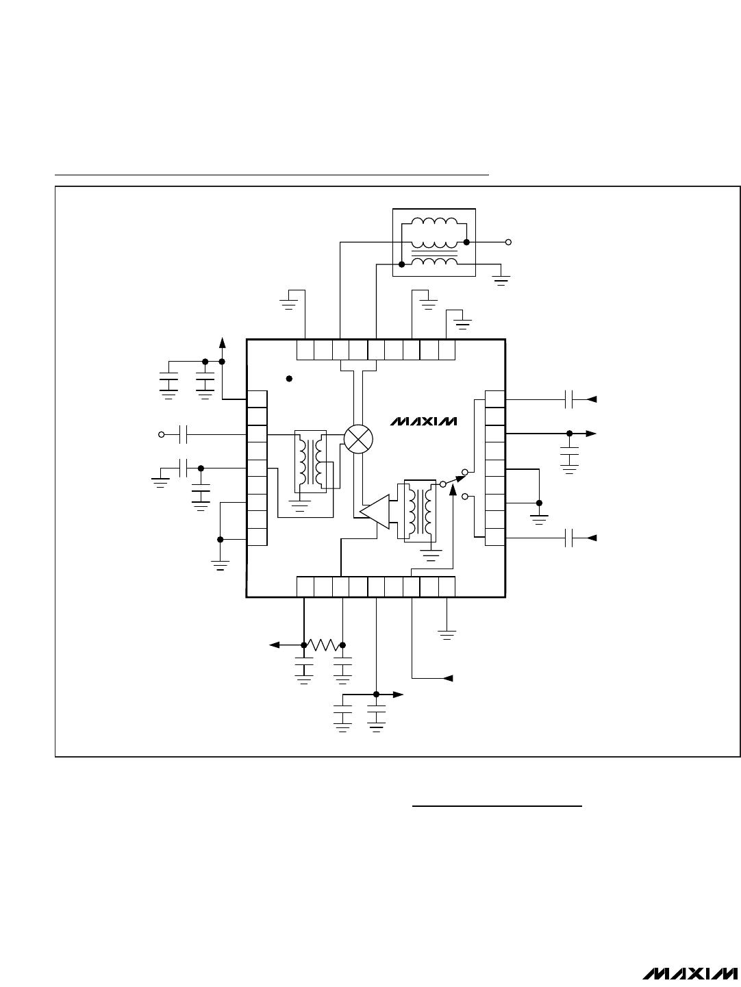
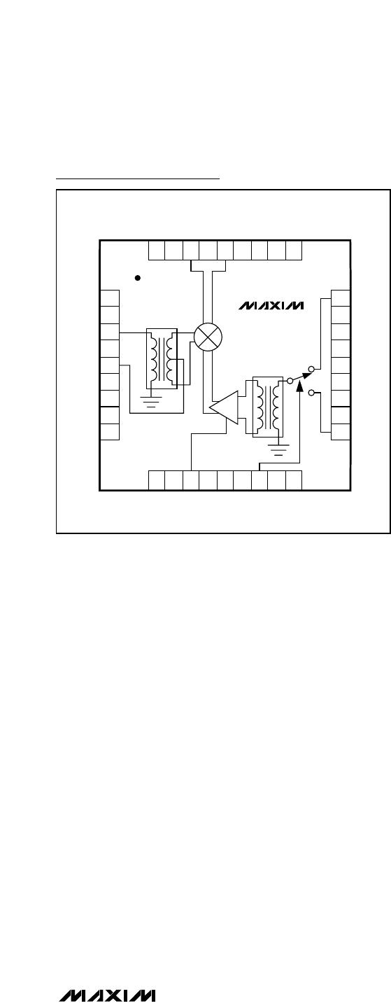
High-Linearity Mixer
The core of the MAX2039 is a double-balanced, high-
performance passive mixer. Exceptional linearity is pro-
vided by the large LO swing from the on-chip LO
buffer.
Differential IF
The MAX2039 mixer has an IF frequency range of DC to
350MHz. Note that these differential ports are ideal for
providing enhanced IIP2 performance. Single-ended IF
applications require a 1:1 balun to transform the 50Ω dif-
ferential IF impedance to a 50Ω single-ended system.
After the balun, the IF return loss is better than 15dB.
The differential IF is used as an input port for upconvert-
er operation. The user can use a differential IF amplifier
following the mixer but a DC block is required on both IF
pins. In this configuration, the IF+ and IF- pins need to
be returned to ground through a high resistance (about
1kΩ). This ground return can also be accomplished by
grounding the RF TAP (pin 3) and AC-coupling the IF+
and IF- ports (pins 19 and 18).
Applications Information
Input and Output Matching
The RF and LO inputs are internally matched to 50Ω. No
matching components are required. Return loss at the RF
port is typically 18dB over the entire input range
(1700MHz to 2200MHz) and return loss at the LO ports is
typically 16dB (1500MHz to 2000MHz). RF and LO inputs
require only DC-blocking capacitors for interfacing.
The IF output impedance is 50Ω (differential). For eval-
uation, an external low-loss 1:1 (impedance ratio) balun
transforms this impedance to a 50Ω single-ended out-
put (see the Typical Application Circuit).
Bias Resistor
Bias current for the LO buffer is optimized by fine tun-
ing resistor R1. If reduced current is required at the
expense of performance, contact the factory for details.
If the ±1% bias resistor values are not readily available,
substitute standard ±5% values.
Layout Considerations
A properly designed PC board is an essential part of
any RF/microwave circuit. Keep RF signal lines as short
as possible to reduce losses, radiation, and induc-
tance. For the best performance, route the ground pin
traces directly to the exposed pad under the package.
The PC board exposed pad MUST be connected to the
ground plane of the PC board. It is suggested that mul-
tiple vias be used to connect this pad to the lower-level
ground planes. This method provides a good RF/ther-
mal conduction path for the device. Solder the exposed
pad on the bottom of the device package to the PC
board. The MAX2039 Evaluation Kit can be used as a
reference for board layout. Gerber files are available
upon request at www.maxim-ic.com.
Power-Supply Bypassing
Proper voltage-supply bypassing is essential for high-
frequency circuit stability. Bypass each V
CC
pin and
TAP with the capacitors shown in the Typical
Application Circuit; see Table 1. Place the TAP bypass
capacitor to ground within 100 mils of the TAP pin.
MAX2039
High-Linearity, 1700MHz to 2200MHz Upconversion/
Downconversion Mixer with LO Buffer/Switch
______________________________________________________________________________________ 13