NCP3520DMR2G

© Semiconductor Components Industries, LLC, 2007
May, 2007 - Rev. 2
1 Publication Order Number:
NCP3520/D
NCP3520/NCP3521
LDO Regulator Controller
The NCP3520 / NCP3521 parts are Low Drop Out (LDO) regulator
controllers for applications requiring high-currents and ultra low
dropout voltages. The use of an external NMOS driver allows the user
to adapt the device to a multitude of applications depending on system
requirements for current and dropout voltage.
Features
Fixed Voltage Options
NCP3520 (1.2 V)
NCP3521 (1.5 V)
Low Operating Current
Low Standby Current (sleep mode < 1 mA)
Non Rush Current on Startup
Short Circuit Protection
1% Output Voltage Tolerance
Drop-In Replacement for Rohm BD3520FVM and BD3521FVM
Functionally Equivalent to Rohm BD3501FVM and BD3502FVM
These are Pb-Free Devices
Typical Applications
Consumer: Set-Top Boxes, Gaming Consoles
LCD Televisions
FPGA
Networking Equipment
Figure 1. Application Diagram
NCP3520
NCP3521
VD
G
VS
VFB
EN
NRCS
GND
VCC
NOTE: For best performance V
FB
should
utilize a Kelvin connection at the load.
10 mF
220 mF
NTMS4107N
or equivalent
V
D
V
O
3.0 A
5.0 V
1.0 mF
0.01 mF
PIN CONNECTIONS
XXXX = 3520 for Fixed 1.2 V or
= 3521 for Fixed 1.5 V
A = Assembly Location
Y = Year
W = Work Week
G = Pb-Free Package
Micro8
DM SUFFIX
CASE 846A
STYLE 2
MARKING
DIAGRAM
1
VD
GND
NRCS
EN
VCC
G
VFB
VS
Micro8
(Top View)
1
2
3
4
8
7
6
5
http://onsemi.com
XXXX
AYWG
G
1
8
(Note: Microdot may be in either location)
See detailed ordering and shipping information in the package
dimensions section on page 9 of this data sheet.
ORDERING INFORMATION
NCP3520/NCP3521
http://onsemi.com
2
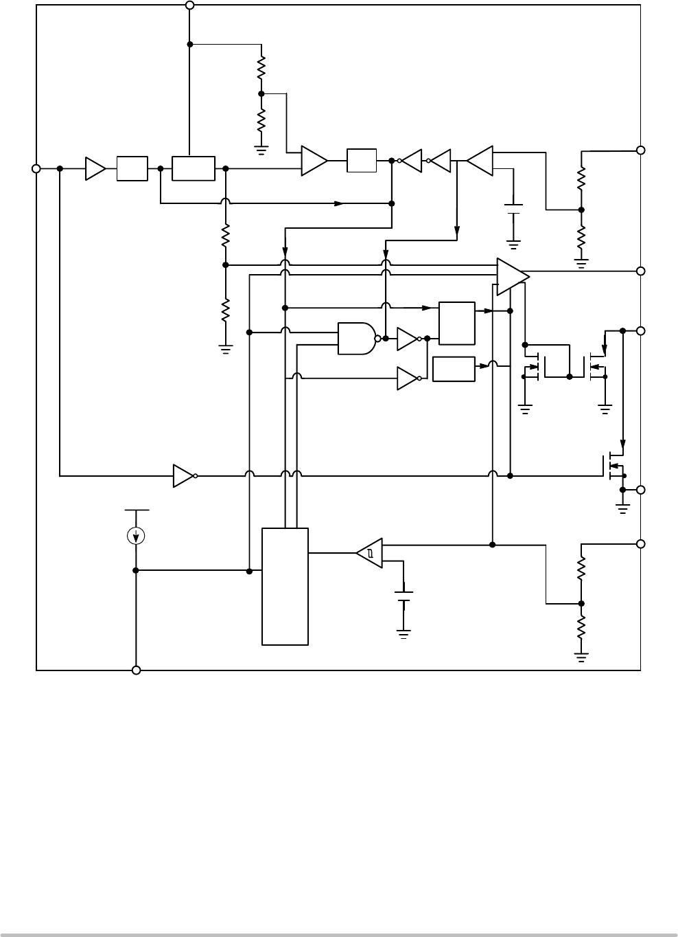
Figure 2. Block Diagram
50ms
Timer
50ms
Timer
-
+
-
+
-
+
+
+
-
+
-
-
+
Voltage
Reference
Output
Off
Latch
Thermal
Shutdown
Latch
Clear
Latch
Set
Non Rush
Current on
Startup
(NRCS)
with 50 ms
Startup
Short
Detect
Short Circuit
Protection
35% of V
OUT
20mA
V
REF
220mA
1.2mA
NRCS
VFB
GND
VS
G
VD
VD_UVLOVCC_UVLO
VCC
EN
0.65V
NCP3520/NCP3521
http://onsemi.com
3
PACKAGE PIN DESCRIPTION Micro8
Pin # Symbol Description
1 NRCS Non Rush current on Startup. Capacitor to ground controls output voltage slew rate and short circuit
delay time.
2 GND Ground.
3 EN Enable input control.
4 VCC Power Supply Voltage Input.
5 VFB Voltage Feedback pin into the error amplifier for maintaining the output voltage.
6 VS Source input. Provides pulldown capability (1.2 mA operating & 220 mA turnoff) for fast output voltage
response time.
7 G Gate Drive for the external NFET.
8 VD NFET Drain input for voltage sensing.
MAXIMUM RATINGS
Rating Value Unit
All Pins -0.3 to 7 V
IG (DC)
IG (AC)
IVS (DC)
10
10
300
mA
Electrostatic Discharge, Human Body Model 1.5 kV
Electrostatic Discharge, Machine Model 100 V
Package Thermal Resistance
Micro8 238 °C/W
Operating Junction Temperature -10 to 150 °C
Storage Temperature Range -55 to 150 °C
Stresses exceeding Maximum Ratings may damage the device. Maximum Ratings are stress ratings only. Functional operation above the
Recommended Operating Conditions is not implied. Extended exposure to stresses above the Recommended Operating Conditions may affect
device reliability.
ELECTRICAL CHARACTERISTICS (T
J
= 25°C, V
CC
= 5 V, V
D
= 2.0 V, EN = 3 V, External FET = NTMS4107N (Note 3), unless
otherwise specified)
Characteristic Conditions Min Typ Max Unit
REGULATOR OUTPUT
Feedback Voltage (NCP3520) I
O
(NTMS4107N) = 50 mA
4.5 V < V
CC
< 5.5 V, 0°C < T
J
< 100°C
(Note 1)
1.188
1.176
1.200
1.200
1.212
1.224
V
V
Feedback Voltage (NCP3521) I
O
(NTMS4107N) = 50 mA
4.5 V < V
CC
< 5.5V, 0°C < T
J
< 100°C
(Note 1)
1.485
1.470
1.500
1.500
1.515
1.530
V
V
Supply Current
Sleep Mode
Run Mode
Short Circuit Latch Condition
EN = 0 V
EN = 3 V
EN = 3 V
-
-
-
0
1.25
0.5
10
1.7
1.7
mA
mA
mA
Line Regulation (NCP3520) 4.5 V < V
CC
< 5.5 V, I
OUT
= 0
4.5 V < V
CC
< 5.5 V, I
OUT
= 3 A (Note 1)
- 1.2
1.2
6.0
6.0
mV
mV
Line Regulation (NCP3521) 4.5 V < V
CC
< 5.5 V, I
OUT
= 0
4.5 V < V
CC
< 5.5 V, I
OUT
= 3 A (Note 1)
- 1.5
1.5
7.5
7.5
mV
mV
Load Regulation (Note 2) I
O
= 0 A to 3 A - 0.50 10 mV
1. Guaranteed by Design
2. Load regulation may vary with the selection of an external FET other than the NTMS4107N.
3. See “External Components” section on Page 8.

NCP3520DMR2G

Mfr. #:
Manufacturer:
ON Semiconductor
Description:
LDO Voltage Controllers LDO REG CONTROLLER 1.2 FIXED VOLTAGE
Lifecycle:
New from this manufacturer.
Delivery:
DHL FedEx Ups TNT EMS
Payment:
T/T Paypal Visa MoneyGram Western Union

Products related to this Datasheet