NCP3520DMR2G

NCP3520/NCP3521
http://onsemi.com
7
DETAILED OPERATING DESCRIPTION
General
The NCP3520/NCP3521 are LDO Regulator Controllers.
An external NFET device sets the current capability
allowing for designer selection.
Features include an undervoltage lockout for both the
integrated circuit supply Pin VCC, and the supply pin for the
external FET connection to the drain of the FET.
The NRCS (Non Rush Current on Startup) feature
prevents high currents through the external FET
(drain-source). The external capacitor setting component
used in NRCS is also used for short circuit protection (SCP).
The device also has an enable feature allowing it to go into
a low supply current sleep mode demanded by most modern
day feature rich systems when not in use.
Thermal shutdown functionality protects the IC from
damage caused from excessively high temperatures
appearing on the IC.
Output Driver
Output current drive capability is determined by the
designer's choice of external MOSFET (NFET). Power
dissipated in the driver can be controlled by the voltage
applied to V
D
. V
D
should be kept low to minimize power
dissipation and high enough to support regulated operation
at the desired output current. It should also be noted the
output capacitor (V
O
to GND) value supports regulation
during high speed transient events until the system loop can
respond to any voltage dips to drive the external FET.
High Speed Control
Unlike most linear regulators whose reaction to
overvoltage events is to turn off the upper driver and let the
external load and resistor feedback network quench the
incident, the NCP3520/21 include a 1.2 mA pulldown
through the VS Pin. This keeps overshoot to a minimum
during powerup. During turn-off and thermal overload, the
pulldown current is increased from 1.2 mA to 220 mA to
provide an even faster turn-off time.
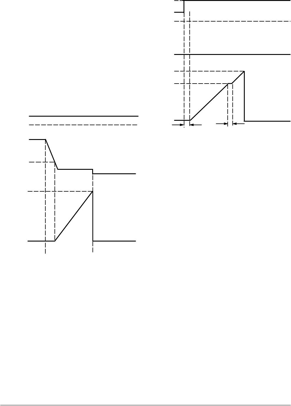
Power On Reset
A 50 ms power on reset circuit is built into the IC acting as
a digital filter and performing housekeeping activity during
a short circuit event.
The timer effects three areas of operation.
1. EN turn on delay. Upon detection of an EN high,
there is a 50 ms delay to when the internal circuitry
turns on and the gate pin (G) goes high. A low on
EN resets the timer.
2. V
CC
startup delay. If V
CC
drops out below the
undervoltage lockout voltage and restored above
its hysteresis value, a 50 ms time is also observed
from reinitiation of V
CC
and G going high. This is
recognized to be different from the EN turn on
delay by the active circuitry of the voltage
reference, NRCS circuitry, and V
S
high current
pulldown.
3. Device startup into a short circuit. Further details
are available on this subject under the heading
“Starting Up Into A Short Circuit”.
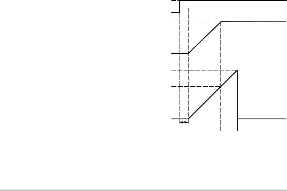
Normal Powerup/Down
The NRCS (Non Rush Current on Startup) timer controls
the output driver during powerup. The output driver voltage
(V
G
) is controlled during powerup. The voltage on NRCS is
mimicked to provide a duplicate voltage on VFB. When
1.2 V is reached normal operation of the error amplifier and
feedback network take over. Regulation is maintained in the
loop around 1.2 V. The NRCS pin rises up to 1 V. At 1 V, the
NRCS capacitor is discharged fully at a 300 mA (min) rate.
The IC enters a standby mode capable of short circuit
detection.
A 20 mA pullup current source is used to charge the
external NRCS capacitor linearly and maintain a predictable
powerup. A recommended 0.01 mF will provide a 325 ms
powerup time. Alternative times can be programmed with
this equation:
T + C(NRCS) * V
FB
ńINRCS
(eq. 1)
Rush current during startup can be calculated by
I = C
OUT
* V
O
/ T.
The NRCS circuit is not active during powerdown.
Normal circuit operation will be maintained unless
VCC_UVLO or VD_UVLO cause the gate drive output to
turn off.
NRCS
1.0 V
VS / VFB
1.2 V
EN
3 V
0.65 V
Figure 13. Powerup (NCP3520 (1.2 V) Version Shown)
A standby mode for
short circuit is
entered here.
Error amplifier
takes control here.
50 ms
NCP3520/NCP3521
http://onsemi.com
8
Short Circuit Protection (SCP)
The IC enters normal mode after the NRCS has gone
through powerup. The NRCS capacitor has reached a 1 V
(typ) threshold and fully discharged (50 mV (max)).
When a short circuit event occurs it is detected when the
voltage on V
FB
goes below (35% of V
OUT
). This triggers the
NRCS current source to start charging the NRCS capacitor
at the same 20 mA rate as during powerup. When the voltage
on the capacitor reaches 1.3 V a short circuit event is
confirmed, V
G
goes low turning off the external FET. V
S
Standby Current pulldown is enabled.
Clearing a Short Circuit Latch Condition
A short circuit latch condition can be cleared by toggling
the EN from its high condition to a low condition, and then
back to a high condition.
Figure 14. Short Circuit (NCP3520 (1.2 V)
Version Shown)
NRCS
1.3 V
VS / VFB
1.2 V
EN
3 V
0 V
V
O
* 0.35
Shirt Circuit
is Detected
Output Falls Out
of Regulation
Output Turns Off
Starting Up Into a Short Circuit
If the NCP3520/NCP3521 turns on and has not gone into
a normal mode of operation, additional time has been added
to the NRCS to ignore potential false short circuit
confirmation during in-rush current events. This time is
independent of the external capacitor value and is typically
50 ms. The voltage on NRCS operates as a normal condition
until it reaches 1 V. The current source charging NRCS turns
off for 50 ms disallowing the voltage to rise on NRCS. After
50 ms the current source turns back on and continues to
charge the NRCS capacitor. Once 1.3 V is reached, the
circuit operates as during a typical short circuit event.
NRCS
1.3 V
VS / VFB
1.2 V
EN
3 V
50 ms
Shirt Circuit Decision Timer
1.0 V
Figure 15. Starting Up Into a Short Circuit (NCP3520
(1.2 V) Version Shown)
50 ms
Undervoltage Lockout
V
CC
and V
D
detection is provided in conjunction with the
EN input pin. When all three conditions are met (V
CC
is up,
V
D
is up, and EN is high), the Non Rush Current on Startup
(NRCS) circuitry is allowed to start. Any one of the three
conditions failing will not allow the device to turn on.
The V
CC
undervoltage threshold is 4.35 V and the V
D
threshold is V
O
* 0.7.
Enable
The Enable function is controlled by the logic pin EN. The
threshold of this pin is set to TTL logic levels. TTL logic
levels are 0.8 V (low) and 2.0 V (high). A low on the EN pin
puts the device is a low current sleep mode consuming less
than 10 mA (I
VCC
). A device going from normal operation
to sleep will 1
st
go through a discharge mode maintaining a
discharge current of 220 mA on V
S
(measured @ V
S
= 1 V).
This pin has 60 mV (typ) of hysteresis to guarantee a clean
switching threshold.
External Components
A capacitor between V
O
and ground is required for
stability. A 220 mF value capacitor such as the
SANYO 2R5TPE220MF is recommended. The
SANYO 2R5TPE220MF capacitor has a 15 mW maximum
specification. Contact resistance and board trace resistance
are the significant contributors to output capacitor ESR
below 10 mW.
As ON Semiconductor's NCP352X family of LDO
controllers may be considered as an alternative to
Rohm's family of LDO controllers, alternative FETs such as
industry compatible parts like the Si4866DY may also be
used in conjunction with ON Semiconductor's controller.
NCP3520/NCP3521
http://onsemi.com
9
Thermal Shutdown
When the die temperature exceeds the Thermal Shutdown
threshold, a Thermal Shutdown (TSD) event is detected and
V
G
is turned off. The IC will remain in this state until the die
temperature moves below the shutdown threshold (180°C
typical) minus the hysteresis factor (15°C typical). The
output will then go through a soft startup using the NRCS
circuitry.
ORDERING INFORMATION
Device Package Shipping
NCP3520DMR2G Micro8
(Pb-Free)
4000 / Tape & Reel
NCP3521DMR2G Micro8
(Pb-Free)
4000 / Tape & Reel
For information on tape and reel specifications, including part orientation and tape sizes, please refer to our Tape and Reel Packaging
Specifications Brochure, BRD8011/D.

NCP3520DMR2G

Mfr. #:
Manufacturer:
ON Semiconductor
Description:
LDO Voltage Controllers LDO REG CONTROLLER 1.2 FIXED VOLTAGE
Lifecycle:
New from this manufacturer.
Delivery:
DHL FedEx Ups TNT EMS
Payment:
T/T Paypal Visa MoneyGram Western Union

Products related to this Datasheet