Expand menu
0
Cart
Home
Products
Sensors
Semiconductors
Passive Components
Connectors
Power
Electromechanical
Optoelectronics
Circuit Protection
Integrated Circuits - ICs
Main Products
Manufacturers
Blog
Services
About OMO
About Us
Contact Us
Check Stock
VNP49N04
P1-P3
P4-P6
P7-P9
P10-P11
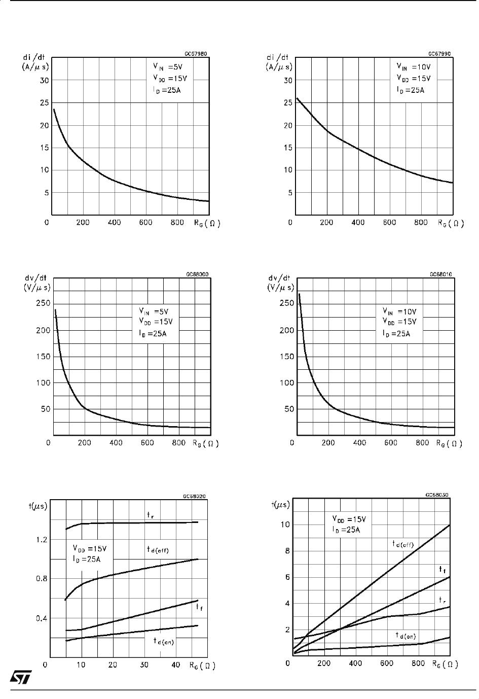
T
urn-
on
Current Slope
T
urn-
off
Drain-S
ource
V
oltage
Slope
Swit
ching
Tim
e Resistiv
e
Load
T
urn-
on
Curr
ent Slope
T
urn-
off D
rain-Source
V
oltage
Slope
Swit
ching
Time
Resisti
ve
Load
VNP49
N04
7/1
1
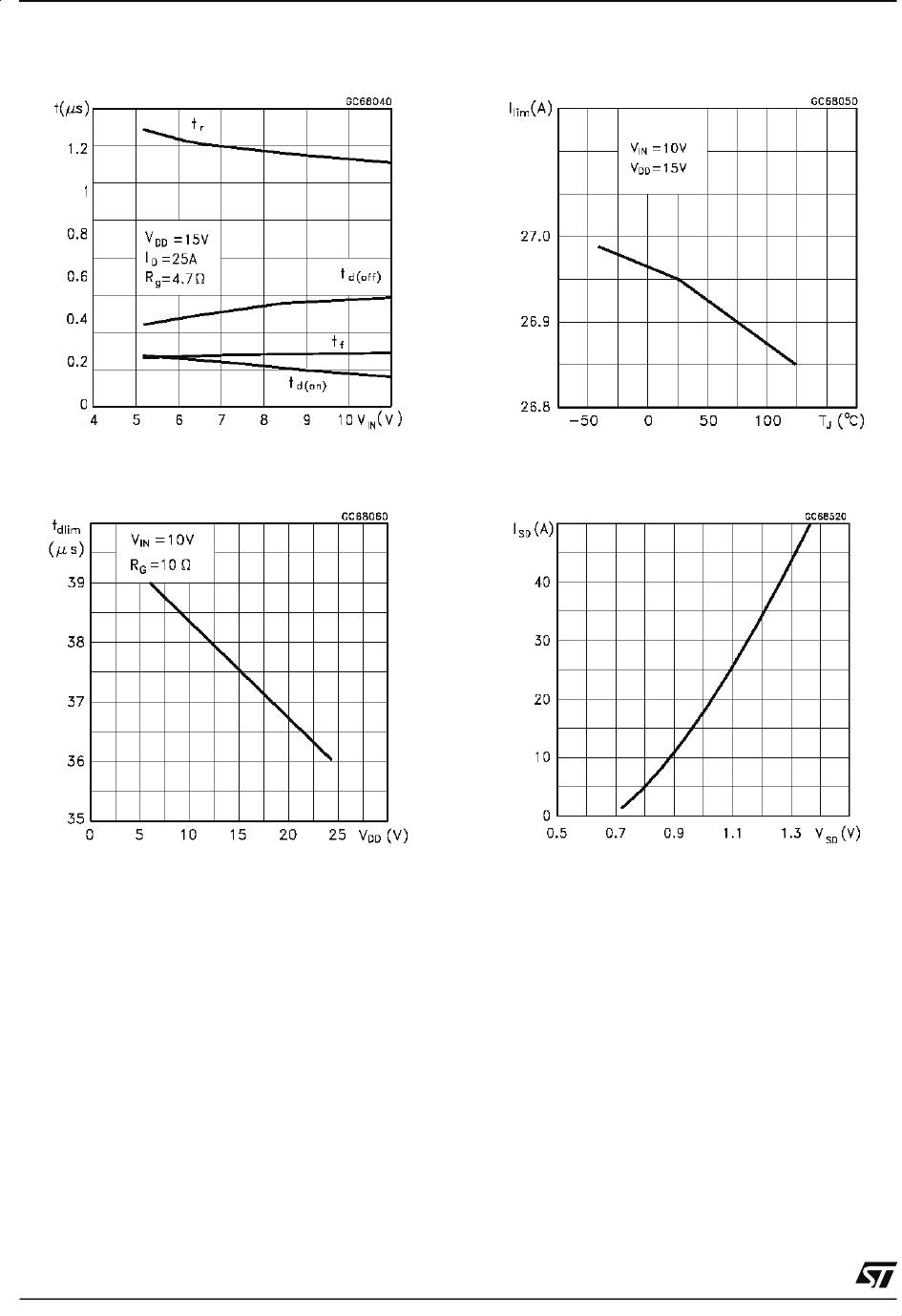
Swit
ching
Tim
e Resistiv
e
Load
Step
Response
Current
Limit
Cur
rent Lim
it
vs Junction
T
emperature
Source
Drain
Diode
Forw
ard
Characteris
tic
s
VNP49N0
4
8/1
1
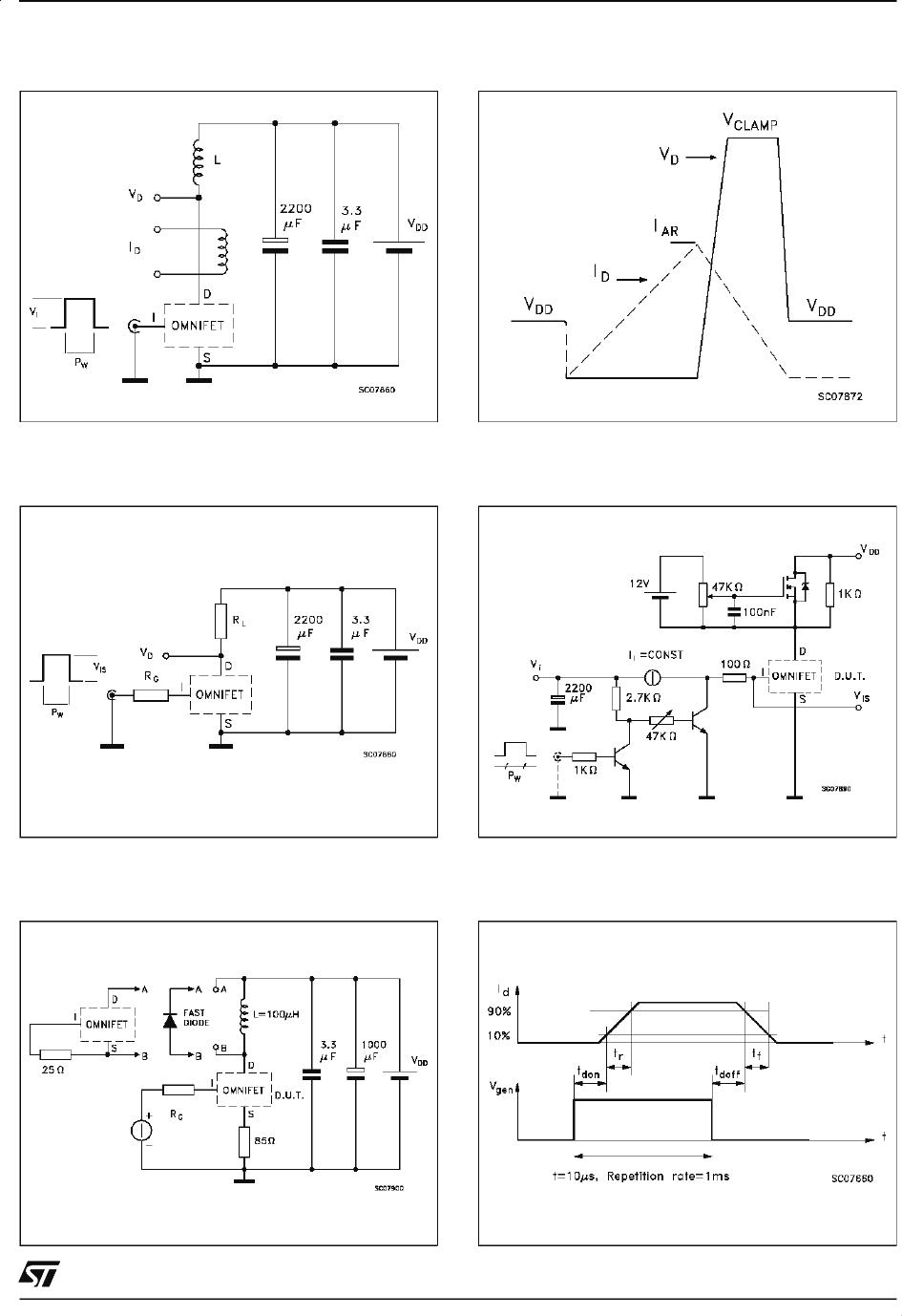
Fig.
2:
Unclam
ped
Inductiv
e
W
aveform
s
Fig.
3:
Switc
hing
T
imes
T
est Circuit
s For
Resist
ive
Load
Fig.
4:
Input
Charge
T
est
Circuit
Fig.
1:
Unclamped
Inductiv
e
Load
T
est
Circ
uits
Fig.
5:
T
est
Circu
it For
Inducti
ve
Load S
witc
hing
And
Di
ode
Recovery
Ti
mes
Fig.
6:
W
avef
orm
s
VNP49
N04
9/1
1
P1-P3
P4-P6
P7-P9
P10-P11
VNP49N04
Mfr. #:
Buy VNP49N04
Manufacturer:
STMicroelectronics
Description:
MOSFET N-Ch 42V 49A OmniFET
Lifecycle:
New from this manufacturer.
Delivery:
DHL
FedEx
Ups
TNT
EMS
Payment:
T/T
Paypal
Visa
MoneyGram
Western
Union
Products related to this Datasheet
VNP49N04-E
VNP49N04