NXP Semiconductors
PMV250EPEA
40 V, P-channel Trench MOSFET
PMV250EPEA All information provided in this document is subject to legal disclaimers. © NXP Semiconductors N.V. 2014. All rights reserved
Product data sheet 20 June 2014 3 / 16
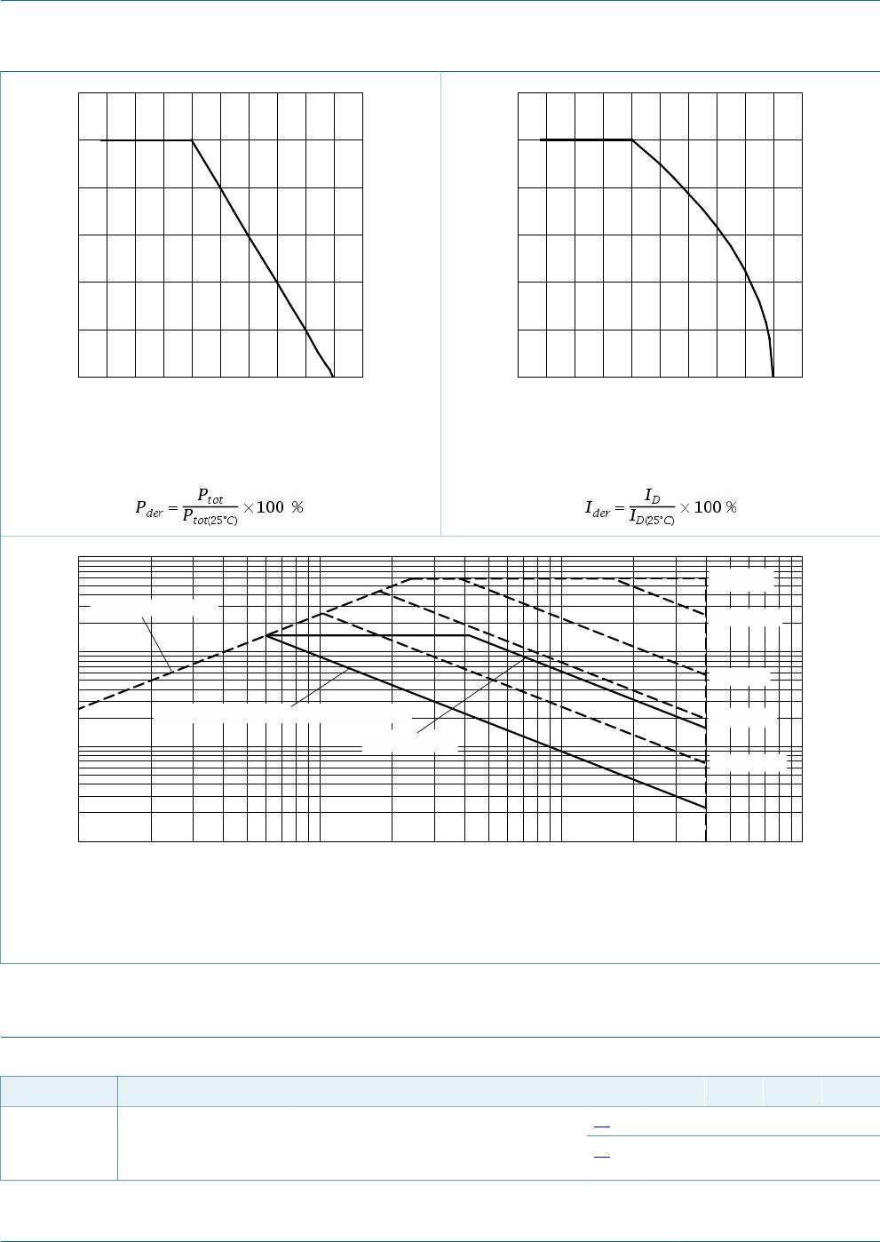
8. Limiting values
Table 5. Limiting values
In accordance with the Absolute Maximum Rating System (IEC 60134).
Symbol Parameter Conditions Min Max Unit
V
DS
drain-source voltage - -40 V
V
GS
gate-source voltage
T
j
= 25 °C
-20 20 V
V
GS
= -10 V; T
amb
= 25 °C [1] - -1.5 AI
D
drain current
V
GS
= -10 V; T
amb
= 100 °C [1] - -1 A
I
DM
peak drain current T
amb
= 25 °C; single pulse; t
p
≤ 10 µs - -6 A
E
DS(AL)S
non-repetitive drain-source
avalanche energy
T
j(init)
= 25 °C; I
D
= -0.26 A; DUT in
avalanche (unclamped)
- 5.5 mJ
[2] - 480 mWT
amb
= 25 °C
[1] - 890 mW
P
tot
total power dissipation
T
sp
= 25 °C - 6250 mW
T
j
junction temperature -55 150 °C
T
amb
ambient temperature -55 150 °C
T
stg
storage temperature -65 150 °C
Source-drain diode
I
S
source current T
amb
= 25 °C [1] - -0.9 A
ESD maximum rating
V
ESD
electrostatic discharge voltage HBM [3] - 1000 V
[1] Device mounted on an FR4 Printed-Circuit Board (PCB), single-sided copper, tin-plated, mounting pad for
drain 6 cm
2
.
[2] Device mounted on an FR4 PCB, single-sided copper, tin-plated and standard footprint.
[3] Measured between all pins.
NXP Semiconductors
PMV250EPEA
40 V, P-channel Trench MOSFET
PMV250EPEA All information provided in this document is subject to legal disclaimers. © NXP Semiconductors N.V. 2014. All rights reserved
Product data sheet 20 June 2014 4 / 16
T
j
(°C)
- 75 17512525 75- 25
017aaa123
40
80
120
P
der
(%)
0
Fig. 1. Normalized total power dissipation as a
function of junction temperature
T
j
(°C)
- 75 17512525 75- 25
017aaa124
40
80
120
I
der
(%)
0
Fig. 2. Normalized continuous drain current as a
function of junction temperature
aaa-011993
V
DS
(V)
-10
-1
-10
2
-10-1
-1
-10
-1
-10
I
D
(A)
-10
-2
t
p
= 100 ms
t
p
= 10 ms
t
p
= 1 ms
t
p
= 100 µs
t
p
= 10 µs
DC; T
amb
= 25 °C; drain mounting pad 6 cm
2
DC; T
sp
= 25 °C
Limit R
DSon
= V
DS
/I
D
I
DM
= single pulse
Fig. 3. Safe operating area; junction to ambient; continuous and peak drain currents as a function of drain-
source voltage
9. Thermal characteristics
Table 6. Thermal characteristics
Symbol Parameter Conditions Min Typ Max Unit
[1] - 230 260 K/WR
th(j-a)
thermal resistance
from junction to
ambient
in free air
[2] - 120 140 K/W
NXP Semiconductors
PMV250EPEA
40 V, P-channel Trench MOSFET
PMV250EPEA All information provided in this document is subject to legal disclaimers. © NXP Semiconductors N.V. 2014. All rights reserved
Product data sheet 20 June 2014 5 / 16
Symbol Parameter Conditions Min Typ Max Unit
R
th(j-sp)
thermal resistance
from junction to solder
point
- 15 20 K/W
[1] Device mounted on an FR4 PCB, single-sided copper, tin-plated and standard footprint.
[2]
Device mounted on an FR4 PCB, single-sided copper, tin-plated, mounting pad for drain 6 cm
2
.
aaa-011994
t
p
(s)
10
-3
10
2
10
3
10110
-2
10
-1
10
2
10
10
3
Z
th(j-a)
(K/W)
1
0
0.02
0.05
0.25
0.33
0.75
duty cycle = 1
0.01
0.50
0.10
0.20
FR4 PCB, standard footprint
Fig. 4. Transient thermal impedance from junction to ambient as a function of pulse duration; typical values
aaa-011995
t
p
(s)
10
-3
10
2
10
3
10110
-2
10
-1
10
2
10
10
3
Z
th(j-a)
(K/W)
1
0
0.02
0.05
0.25
0.33
0.75
duty cycle = 1
0.01
0.50
0.10
0.20
FR4 PCB, mounting pad for drain 6 cm
2
Fig. 5. Transient thermal impedance from junction to ambient as a function of pulse duration; typical values

PMV250EPEAR

Mfr. #:
Manufacturer:
Nexperia
Description:
MOSFET 40V P-channel Trench MOSFET
Lifecycle:
New from this manufacturer.
Delivery:
DHL FedEx Ups TNT EMS
Payment:
T/T Paypal Visa MoneyGram Western Union

Products related to this Datasheet