NXP Semiconductors
PMV250EPEA
40 V, P-channel Trench MOSFET
PMV250EPEA All information provided in this document is subject to legal disclaimers. © NXP Semiconductors N.V. 2014. All rights reserved
Product data sheet 20 June 2014 8 / 16
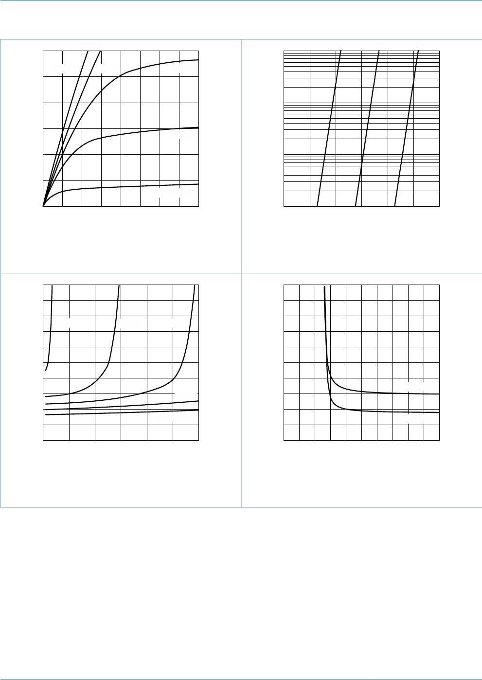
V
GS
(V)
0 -5-4-2 -3-1
aaa-012000
-2
-4
-6
I
D
(A)
0
T
j
= 150 °C T
j
= 25 °C
V
DS
> I
D
× R
DSon
Fig. 10. Transfer characteristics: drain current as a
function of gate-source voltage; typical values
T
j
(°C)
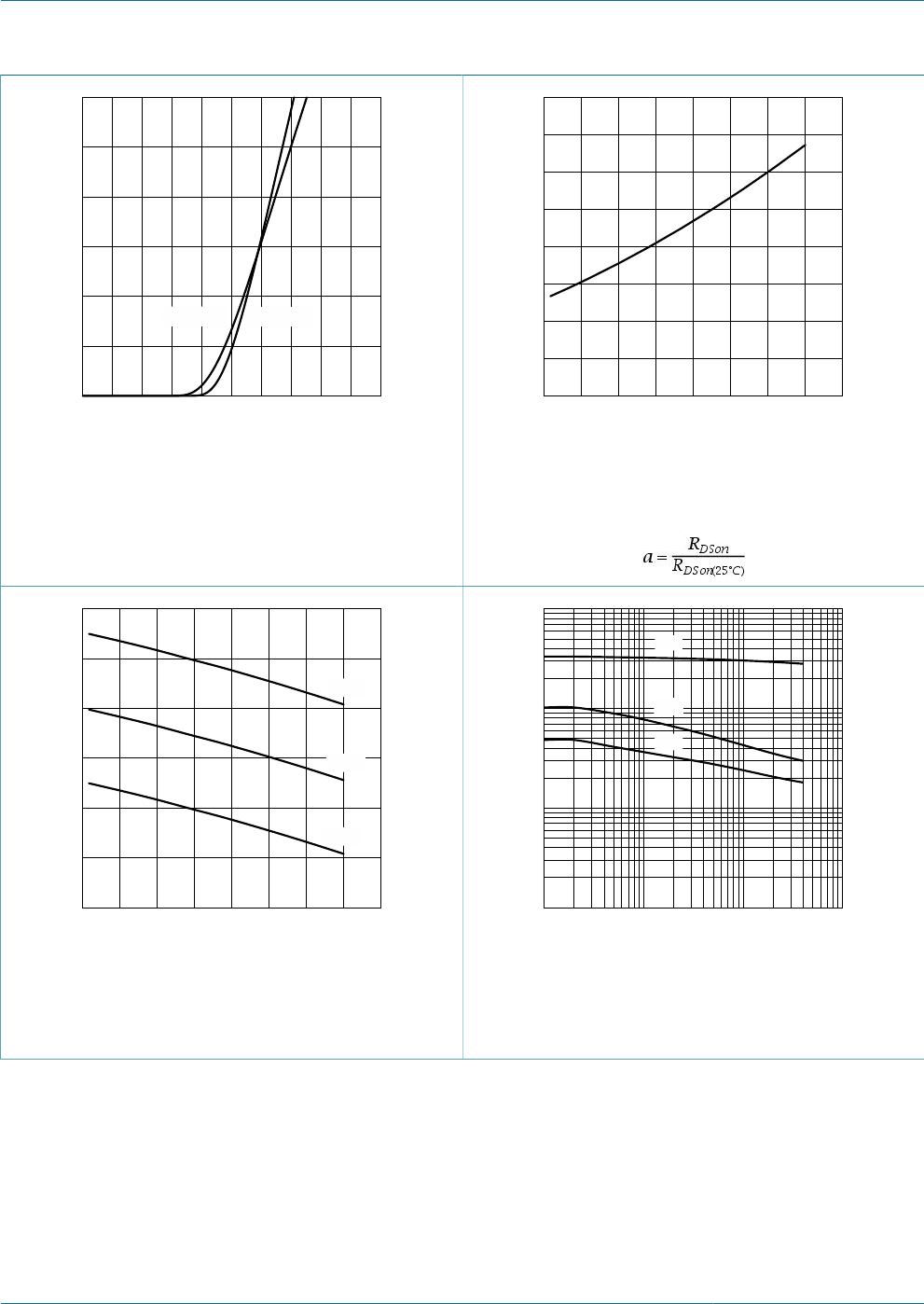
-60 1801200 60
aaa-012001
1.0
0.5
1.5
2.0
a
0
Fig. 11. Normalized drain-source on-state resistance
as a function of junction temperature; typical
values
T
j
(°C)
-60 1801200 60
aaa-012002
-1
-2
-3
V
GS(th)
(V)
0
min
typ
max
I
D
= -0.25 mA; V
DS
= V
GS
Fig. 12. Gate-source threshold voltage as a function of
junction temperature
V
DS
(V)
10
-1
-10
2
-10-1
aaa-012003
10
2
10
10
3
C
(pF)
1
C
iss
C
oss
C
rss
f = 1 MHz; V
GS
= 0 V
Fig. 13. Input, output and reverse transfer capacitances
as a function of drain-source voltage; typical
values