PROGRAMMABLE CLOCK GENERATOR 22 MARCH 3, 2017
5P49V5901 DATASHEET
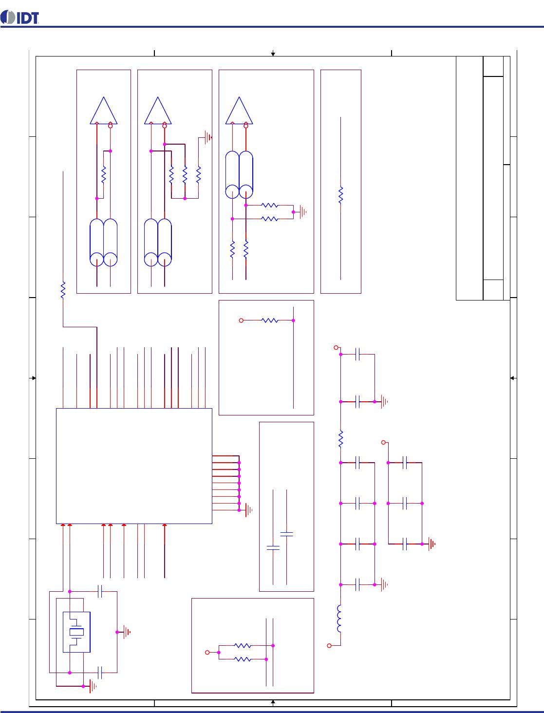
5P49V5901 Application Schematic
The following figure shows an example of 5P49V5901 application schematic. Input and output terminations shown are intended as examples
only and may not represent the exact user configuration. In this example, the device is operated at V
DDD,
V
DDA
= 3.3V. The decoupling
capacitors should be located as close as possible to the power pin. A 12pF parallel resonant 8MHz to 40MHz crystal is used in this example.
Different crystal frequencies may be used. The C1 = C2 = 5pF are recommended for frequency accuracy. If different crystal types are used,
please consult IDT for recommendations. For different board layout, the C1 and C2 may be slightly adjusted for optimizing frequency accuracy.
As with any high speed analog circuitry, the power supply pins are vulnerable to random noise. To achieve optimum jitter performance, power
supply isolation is required. 5P49V5901 provides separate power supplies to isolate any high switching noise from coupling into the internal
PLL.
In order to achieve the best possible filtering, it is recommended that the placement of the filter components be on the device side of the PCB
as close to the power pins as possible. If space is limited, the 0.1uf capacitor in each power pin filter should be placed on the device side. The
other components can be on the opposite side of the PCB.
Power supply filter recommendations are a general guideline to be used for reducing external noise from coupling into the devices. The filter
performance is designed for a wide range of noise frequencies. This low-pass filter starts to attenuate noise at approximately 10 kHz. If a
specific frequency noise component is known, such as switching power supply frequencies, it is recommended that component values be
adjusted and if required, additional filtering be added. Additionally, good general design practices for power plane voltage stability suggests
adding bulk capacitance in the local area of all devices.
The schematic example focuses on functional connections and is not configuration specific. Refer to the pin description and functional tables
in the datasheet to ensure the logic control inputs are properly set.
MARCH 3, 2017 23 PROGRAMMABLE CLOCK GENERATOR
5P49V5901 DATASHEET
5P49V5901 Reference Schematic
8
8
7
7
6
6
5
5
4
4
3
3
2
2
1
1
D D
C C
B B
A A
Layout notes:
1. Separate Xout and Xin Traces by 3 x the trace width
2. Do not share crystal load capacitor ground via with
other components.
3. Route power from bead through bulk capacitor pad
then through 0.1uF capacitor pad then to clock chip
Vdd pad.
4. Do not share ground vias. One ground pin one ground
via.
Revision history
0.1 9/19/2014 first publication
0.2 3/9/2015 correct the LVDS and LVCMOS terminations
Manufacture Part Number Z@100MHz PkgSz DC res. Current(Ma)
Fair-Rite 2504021217Y0 120 0402 0.5 200
muRata BLM15AG221SN1 220 0402 0.35 300
muRata BLM15BB121SN1 120 0402 0.35 300
TDK MMZ1005S241A 240 0402 0.18 200
TECSTAR TB4532153121 120 0402 0.3 300
NOTE:FERRITE BEAD FB1 =
PLACE NEAR
I2C CONTROLLER
IF USED
LVDS TERMINATION
3.3V LVPECL TERMINATION
2.5V and 3.3V HCSL TERMINATION
CONFIGURATION
PULL-UP FOR
HARDWARE
CONTROL
REMOVE FOR I2C
LVCMOS TERMINATION
FOR LVDS, LVPECL AC COUPLE
USE TERMINATION ON RIGHT
FG_X1
V1P8VCA
OUT_0_SEL-I2C
V1P8VC
V1P8VC
OUTR0
CLKIN
CLKINB V1P8VC
OUTR1
CLKSEL OUTRB1
SDA V1P8VC
SCL OUTR2
OUTRB2
SD/OE V1P8VC
OUTR3
OUTRB3
V1P8VC
OUTR4
OUTRB4
SDA
SCL CLKIN
CLKINB
OUT_0_SEL-I2C
V1P8VCA OUTR2
OUT_2
FG_X2
V1P8VC
V1P8VCA
V1P8VC
VCC1P8
V3P3
V1P8VC
Size
Document Number Rev
Date: Sheet
of
0.2
Integrated Device Technology
A
11Monday, March 09, 2015
5P49V5901_SCH
San Jose, CA
Size
Document Number Rev
Date: Sheet
of
0.2
Integrated Device Technology
A
11Monday, March 09, 2015
5P49V5901_SCH
San Jose, CA
Size
Document Number Rev
Date: Sheet
of
0.2
Integrated Device Technology
A
11Monday, March 09, 2015
5P49V5901_SCH
San Jose, CA
R2
2.2
1 2
R3 100
1 2
U2
RECEIVER
1
2
FB1
SIGNAL_BEAD
1 2
C11
.1uF
12
R9
10K
1 2
R12 50
1 2
C8
.1uF
12
C5
.1uF
12
C10
.1uF
12
R5
49.9
1%
1 2
U4
RECEIVER
1
2
C9
.1uF
12
C13 .1uF
1 2
C4
.1uF
12
R14 33
1 2
R10 50
1 2
R11 50
1 2
R8
10K
1 2
U1
5P49V5901
XOUT
3
XIN/REF
4
CLKIN
1
CLKINB
2
CLKSEL
6
SEL1/SDA
8
SEL0/SCL
9
SD/OE
7
VDDA
5
VDDD
22
VDDO0
23
OUT0_SEL_I2CB
24
VDDO1
21
OUT1
20
OUT1B
19
VDDO2
18
OUT2
17
OUT2B
16
VDDO3
15
OUT3
14
OUT3B
13
VDDO4
10
OUT4
11
OUT4B
12
EPAD
25
EPAD
26
EPAD
27
EPAD
28
EPAD
29
EPAD
30
EPAD
31
EPAD
32
EPAD
33
R6 33
1 2
R4
49.9
1%
1 2
C3
.1uF
12
C7
NP
12
C1
10uF
12
R15 33
1 2
R13 33
1 2
GNDGND
Y1
25.000 MHz
CL = 8pF
4
1
2
3
R7
10K
1 2
C6
NP
12
C12 .1uF
1 2
U3
RECEIVER
1
2
C2
1uF
12
25.000MHz
CL=8pF
PROGRAMMABLE CLOCK GENERATOR 24 MARCH 3, 2017
5P49V5901 DATASHEET
Overdriving the XIN/REF Interface
LVCMOS Driver
The XIN/REF input can be overdriven by an LVCMOS driver
or by one side of a differential driver through an AC coupling
capacitor. The XOUT pin can be left floating. The amplitude of
the input signal should be between 500mV and 1.2V and the
slew rate should not be less than 0.2V/ns. Figure General
Diagram for LVCMOS Driver to XTAL Input Interface shows an
example of the interface diagram for a LVCMOS driver.
This configuration has three properties; the total output
impedance of Ro and Rs matches the 50 ohm transmission
line impedance, the Vrx voltage is generated at the CLKIN
inputs which maintains the LVCMOS driver voltage level
across the transmission line for best S/N and the R1-R2
voltage divider values ensure that the clock level at XIN is less
than the maximum value of 1.2V.
General Diagram for LVCMOS Driver to XTAL Input Interface
Table 25 Nominal Voltage Divider Values vs LVCMOS VDD for
XIN
shows resistor values that ensure the maximum drive
level for the XIN/REF port is not exceeded for all combinations
of 5% tolerance on the driver VDD, the VersaClock VDDA and
5% resistor tolerances. The values of the resistors can be
adjusted to reduce the loading for slower and weaker
LVCMOS driver by increasing the voltage divider attenuation
as long as the minimum drive level is maintained over all
tolerances. To assist this assessment, the total load on the
driver is included in the table.
Table 25: Nominal Voltage Divider Values vs LVCMOS VDD for XIN
XOUT
XIN / REF
R1
R2
C3
0. 1 uF
V_XIN
LV CMOS
VDD
Ro
Ro + Rs = 50 ohms
Rs Zo = 50 Ohm
LVCMOS Driver VDD Ro+Rs R1 R2 V_XIN (peak) Ro+Rs+R1+R2
3.3 50.0 130 75 0.97 255
2.5 50.0 100 100 1.00 250
1.8 50.0 62 130 0.97 242

5P49V5901B067NLGI8

Mfr. #:
Manufacturer:
IDT
Description:
Clock Generators & Support Products VersaClock 5 LP Program CLK
Lifecycle:
New from this manufacturer.
Delivery:
DHL FedEx Ups TNT EMS
Payment:
T/T Paypal Visa MoneyGram Western Union