PROGRAMMABLE CLOCK GENERATOR 32 MARCH 3, 2017
5P49V5901 DATASHEET
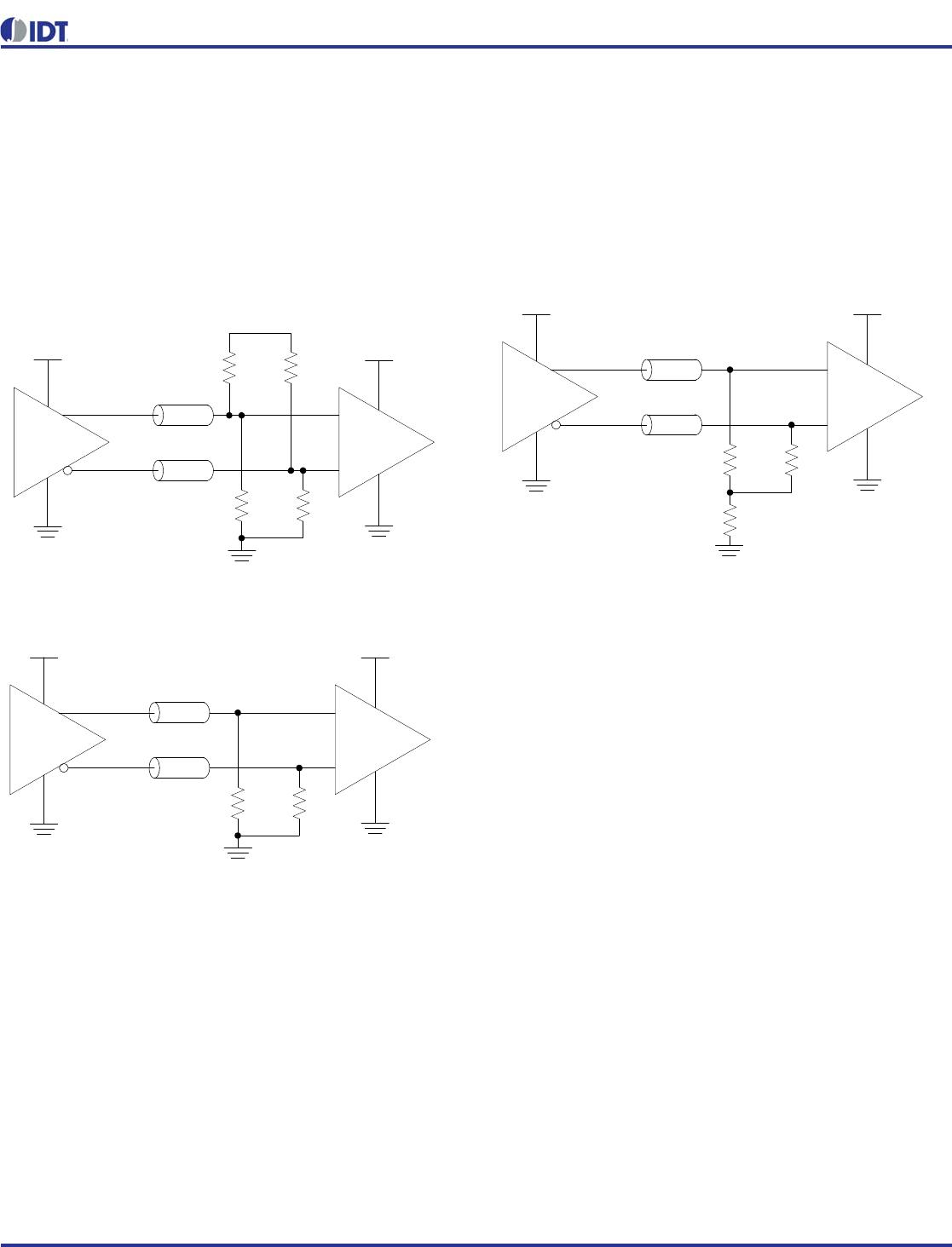
PCI Express Application Note
PCI Express jitter analysis methodology models the system
response to reference clock jitter. The block diagram below
shows the most frequently used Common Clock Architecture
in which a copy of the reference clock is provided to both ends
of the PCI Express Link.
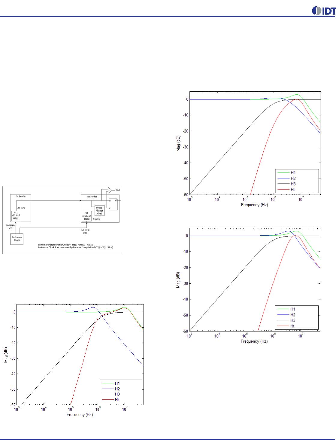
In the jitter analysis, the transmit (Tx) and receive (Rx) serdes
PLLs are modeled as well as the phase interpolator in the
receiver. These transfer functions are called H1, H2, and H3
respectively. The overall system transfer function at the
receiver is:
The jitter spectrum seen by the receiver is the result of
applying this system transfer function to the clock spectrum
X(s) and is:
In order to generate time domain jitter numbers, an inverse
Fourier Transform is performed on X(s)*H3(s) * [H1(s) -
H2(s)].
PCI Express Common Clock Architecture
For PCI Express Gen 1, one transfer function is defined and the
evaluation is performed over the entire spectrum: DC to Nyquist (e.g
for a 100MHz reference clock: 0Hz – 50MHz) and the jitter result is
reported in peak-peak.
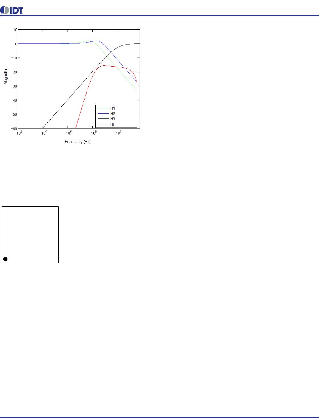
PCIe Gen1 Magnitude of Transfer Function
For PCI Express Gen2, two transfer functions are defined with 2
evaluation ranges and the final jitter number is reported in RMS. The
two evaluation ranges for PCI Express Gen 2 are 10kHz – 1.5MHz
(Low Band) and 1.5MHz – Nyquist (High Band). The plots show the
individual transfer functions as well as the overall transfer function Ht.
PCIe Gen2A Magnitude of Transfer Function
PCIe Gen2B Magnitude of Transfer Function
For PCI Express Gen 3, one transfer function is defined and the
evaluation is performed over the entire spectrum. The transfer
function parameters are different from Gen 1 and the jitter result is
reported in RMS.
Ht s H3 s H1 s H2 s–=
Ys Xs H3 s H1 s H2 s–=