74LCX541MTCX

TC7SZ125FU
1
CMOS Digital Integrated Circuits Silicon Monolithic
TC7SZ125FU
TC7SZ125FU
TC7SZ125FU
TC7SZ125FU
Start of commercial production
1998-08
1.
1.
1.
1. Functional Description
Functional Description
Bus Buffer with 3-State Output
2.
2.
2.
2. Features
Features
Features
Features
(1) AEC-Q100 (Rev. H) (Note 1)
(2) Wide operating temperature range: T
opr
= -40 to 125 (Note 2)
(3) High output current: ±24 mA (min) at V
CC
= 3.0 V
(4) Super high speed operation: t
pd
= 2.6 ns (typ.) at V
CC
= 5.0 V, C
L
= 50 pF
(5) Operation voltage range: V
CC
= 1.65 to 5.5 V
(6) 5.5 V tolerant inputs
(7) 5.5 V power down protection output
(8) Matches the performance of TC74LCX series when operated at 3.3 V V
CC
Note 1: This device is compliant with the reliability requirements of AEC-Q100. For details, contact your Toshiba sales
representative.
Note 2: For devices with the ordering part number TC7SZ125FU,LJ(CT. T
opr
= -40 to 85 for the other devices.
3.
3.
3.
3. Packaging
Packaging
Packaging
Packaging
USV
2016-09-15
Rev.2.0
©2015 Toshiba Corporation
TC7SZ125FU
2
4.
4.
4.
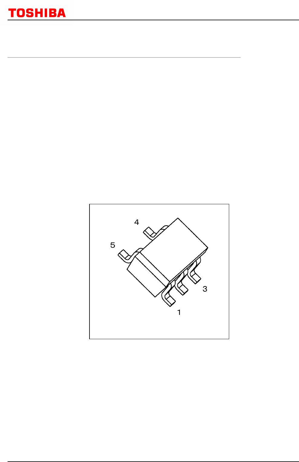
4. Marking and Pin Assignment
Marking and Pin Assignment
Marking
Marking
Marking
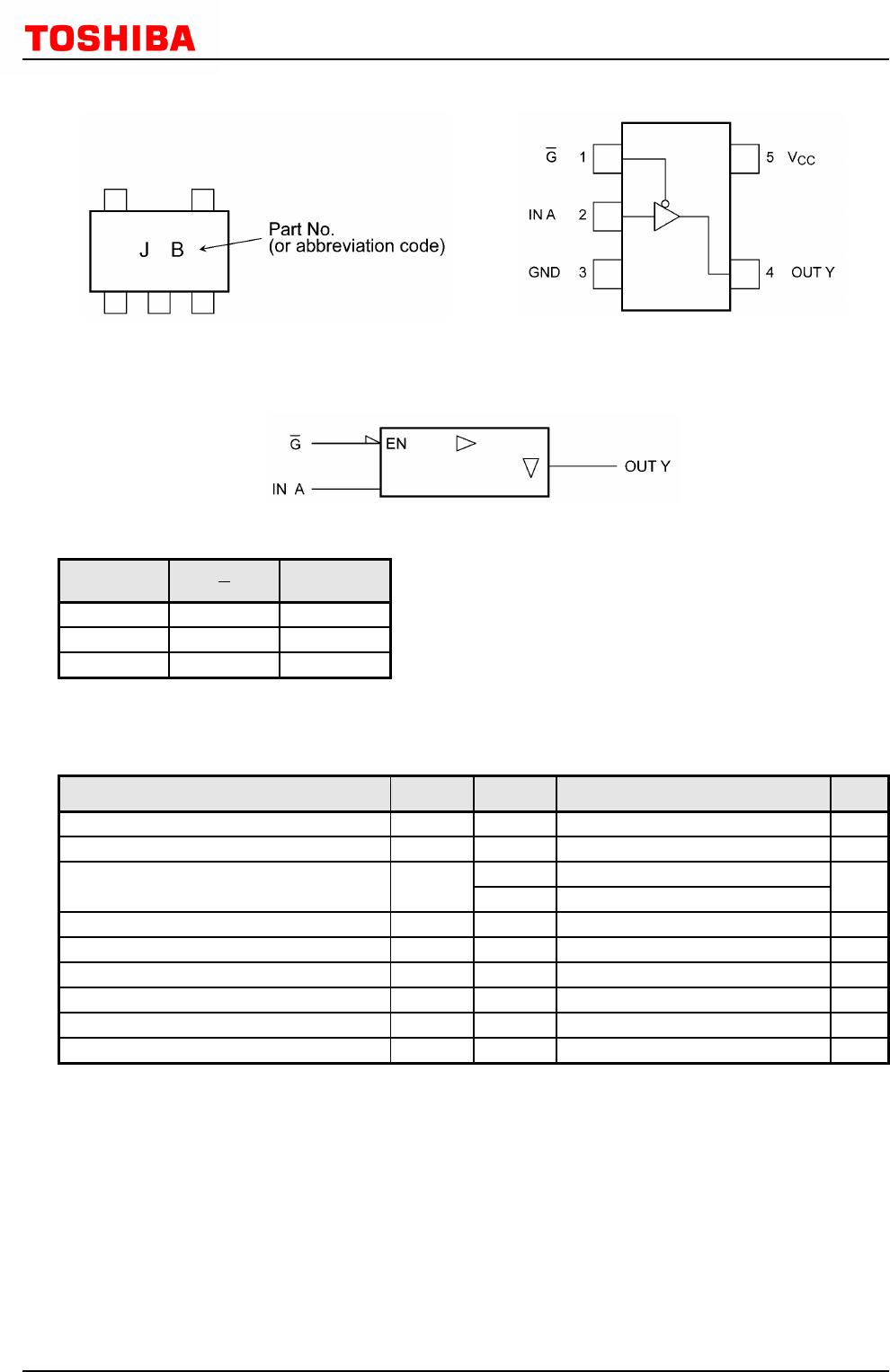
Marking Pin Assignment (Top view)
Pin Assignment (Top view)
5.
5.
5.
5. IEC Logic Symbol
IEC Logic Symbol
IEC Logic Symbol
IEC Logic Symbol
6.
6.
6.
6. Truth Table
Truth Table
Truth Table
Truth Table
Input
A
X
L
H
Input
G
H
L
L
Output
Y
Z
L
H
X: Don't care
Z: High impedance
7.
7.
7.
7. Absolute Maximum Ratings (Note) (Unless otherwise specified, T
Absolute Maximum Ratings (Note) (Unless otherwise specified, T
a
a
a
a
= 25
= 25
= 25
= 25
)
)
)
)
Characteristics
Supply voltage
Input voltage
DC output voltage
Input diode current
Output diode current
DC output current
V
CC
/ground current
Power dissipation
Storage temperature
Symbol
V
CC
V
IN
V
OUT
I
IK
I
OK
I
OUT
I
CC
P
D
T
stg
Note
(Note 1)
(Note 2)
(Note 3)
Rating
-0.5 to 6.0
-0.5 to 6.0
-0.5 to 6.0
-0.5 to V
CC
+ 0.5
-20
-20
±50
±50
200
-65 to 150
Unit
V
V
V
mA
mA
mA
mA
mW
Note: Exceeding any of the absolute maximum ratings, even briefly, lead to deterioration in IC performance or even
destruction.
Using continuously under heavy loads (e.g. the application of high temperature/current/voltage and the
significant change in temperature, etc.) may cause this product to decrease in the reliability significantly even
if the operating conditions (i.e. operating temperature/current/voltage, etc.) are within the absolute maximum
ratings and the operating ranges.
Please design the appropriate reliability upon reviewing the Toshiba Semiconductor Reliability Handbook
(“Handling Precautions”/“Derating Concept and Methods”) and individual reliability data (i.e. reliability test report
and estimated failure rate, etc).
Note 1: V
CC
= 0 V or high impedance condition
Note 2: High (H) or Low (L) state. I
OUT
absolute maximum rating must be observed.
Note 3: V
OUT
< GND
2016-09-15
Rev.2.0
©2015 Toshiba Corporation
TC7SZ125FU
3
8.
8.
8.
8. Operating Ranges (Note)
Operating Ranges (Note)
Characteristics
Supply voltage
Input voltage
Output voltage
Operating temperature
Input rise and fall time
Symbol
V
CC
V
IN
V
OUT
T
opr
dt/dv
Note
(Note 1)
(Note 2)
(Note 3)
(Note 4)
(Note 5)
Test Condition
V
CC
= 1.8 ± 0.15 V, 2.5 ± 0.2 V
V
CC
= 3.3 ± 0.3 V
V
CC
= 5.0 ± 0.5 V
Rating
1.65 to 5.5
1.5 to 5.5
0 to 5.5
0 to 5.5
0 to V
CC
-40 to 125
-40 to 85
0 to 20
0 to 10
0 to 5
Unit
V
V
V
ns/V
Note: The operating ranges must be maintained to ensure the normal operation of the device.
Unused inputs must be tied to either V
CC
or GND.
Note 1: Data retention only
Note 2: V
CC
= 0 V or high impedance condition
Note 3: High (H) or Low (L) state.
Note 4: For devices with the ordering part number TC7SZ125FU,LJ(CT.
Note 5: For devices except those with the ordering part number TC7SZ125FU,LJ(CT.
9.
9.
9.
9. Electrical Characteristics
Electrical Characteristics
9.1.
9.1.
9.1.
9.1. DC Characteristics (Unless otherwise specified, T
DC Characteristics (Unless otherwise specified, T
a
a
a
a
= 25
= 25
= 25
= 25
)
)
)
)
Characteristics
High-level input voltage
Low-level input voltage
High-level output voltage
Low-level output voltage
Input leakage current
3-state output OFF-state
leakage current
Power-OFF leakage
current
Quiescent supply current
Symbol
V
IH
V
IL
V
OH
V
OL
I
IN
I
OZ
I
OFF
I
CC
Test Condition
V
IN
= V
IH
or V
IL
V
IN
= V
IL
V
IN
= 5.5 V or GND
V
IN
= V
IH
or V
IL
V
OUT
= 0 to 5.5 V
V
IN
or V
OUT
= 5.5 V
V
IN
= V
CC
or GND
I
OH
= -100 µA
I
OH
= -8 mA
I
OH
= -16 mA
I
OH
= -24 mA
I
OH
= -32 mA
I
OL
= 100 µA
I
OL
= 8 mA
I
OL
= 16 mA
I
OL
= 24 mA
I
OL
= 32 mA
V
CC
(V)
1.65 to
1.95
2.3 to 5.5
1.65 to
1.95
2.3 to 5.5
1.65
2.3
3.0
4.5
2.3
3.0
3.0
4.5
1.65
2.3
3.0
4.5
2.3
3.0
3.0
4.5
0 to 5.5
1.65 to 5.5
0
5.5
Min
V
CC
× 0.88
V
CC
× 0.75
1.55
2.2
2.9
4.4
1.9
2.4
2.3
3.8
Typ.
1.65
2.3
3.0
4.5
2.15
2.8
2.68
4.2
0.0
0.0
0.0
0.0
0.1
0.15
0.22
0.22
Max
V
CC
× 0.12
V
CC
× 0.25
0.1
0.1
0.1
0.1
0.3
0.4
0.55
0.55
±1.0
±1.0
1
2
Unit
V
V
V
V
µA
µA
µA
µA
2016-09-15
Rev.2.0
©2015 Toshiba Corporation

74LCX541MTCX

Mfr. #:
Manufacturer:
ON Semiconductor / Fairchild
Description:
Buffers & Line Drivers Octal Buff/Line Drv
Lifecycle:
New from this manufacturer.
Delivery:
DHL FedEx Ups TNT EMS
Payment:
T/T Paypal Visa MoneyGram Western Union

Products related to this Datasheet