74LCX541MTCX

TC7SZ125FU
4
9.2.
9.2.
9.2.
9.2. DC Characteristics (Unless otherwise specified, T
DC Characteristics (Unless otherwise specified, T
a
a
a
a
= -40 to 85
= -40 to 85
= -40 to 85
= -40 to 85
)
)
)
)
Characteristics
High-level input voltage
Low-level input voltage
High-level output voltage
Low-level output voltage
Input leakage current
3-state output OFF-state
leakage current
Power-OFF leakage current
Quiescent supply current
Symbol
V
IH
V
IL
V
OH
V
OL
I
IN
I
OZ
I
OFF
I
CC
Test Condition
V
IN
= V
IH
or V
IL
V
IN
= V
IL
V
IN
= 5.5 V or GND
V
IN
= V
IH
or V
IL
V
OUT
= 0 to 5.5 V
V
IN
or V
OUT
= 5.5 V
V
IN
= V
CC
or GND
I
OH
= -100 µA
I
OH
= -8 mA
I
OH
= -16 mA
I
OH
= -24 mA
I
OH
= -32 mA
I
OL
= 100 µA
I
OL
= 8 mA
I
OL
= 16 mA
I
OL
= 24 mA
I
OL
= 32 mA
V
CC
(V)
1.65 to
1.95
2.3 to 5.5
1.65 to
1.95
2.3 to 5.5
1.65
2.3
3.0
4.5
2.3
3.0
3.0
4.5
1.65
2.3
3.0
4.5
2.3
3.0
3.0
4.5
0 to 5.5
1.65 to 5.5
0
5.5
Min
V
CC
× 0.88
V
CC
× 0.75
1.55
2.2
2.9
4.4
1.9
2.4
2.3
3.8
Max
V
CC
× 0.12
V
CC
× 0.25
0.1
0.1
0.1
0.1
0.3
0.4
0.55
0.55
±10.0
±10.0
10
20
Unit
V
V
V
V
µA
µA
µA
µA
2016-09-15
Rev.2.0
©2015 Toshiba Corporation
TC7SZ125FU
5
9.3.
9.3.
9.3.
9.3. DC Characteristics (Note) (Unless otherwise specified, T
DC Characteristics (Note) (Unless otherwise specified, T
a
a
a
a
= -40 to 125
= -40 to 125
= -40 to 125
= -40 to 125
)
)
)
)
Characteristics
High-level input voltage
Low-level input voltage
High-level output voltage
Low-level output voltage
Input leakage current
3-state output OFF-state
leakage current
Power-OFF leakage current
Quiescent supply current
Symbol
V
IH
V
IL
V
OH
V
OL
I
IN
I
OZ
I
OFF
I
CC
Test Condition
V
IN
= V
IH
or V
IL
V
IN
= V
IL
V
IN
= 5.5 V or GND
V
IN
= V
IH
or V
IL
V
OUT
= 0 to 5.5 V
V
IN
or V
OUT
= 5.5 V
V
IN
= V
CC
or GND
I
OH
= -100 µA
I
OH
= -8 mA
I
OH
= -16 mA
I
OH
= -24 mA
I
OH
= -32 mA
I
OL
= 100 µA
I
OL
= 8 mA
I
OL
= 16 mA
I
OL
= 24 mA
I
OL
= 32 mA
V
CC
(V)
1.65 to
1.95
2.3 to 5.5
1.65 to
1.95
2.3 to 5.5
1.65
2.3
3.0
4.5
2.3
3.0
3.0
4.5
1.65
2.3
3.0
4.5
2.3
3.0
3.0
4.5
0 to 5.5
1.65 to 5.5
0
5.5
Min
V
CC
× 0.88
V
CC
× 0.75
1.55
2.2
2.9
4.4
1.7
2.2
2.0
3.4
Max
V
CC
× 0.12
V
CC
× 0.25
0.1
0.1
0.1
0.1
0.45
0.6
0.8
0.8
±20.0
±20.0
100
200
Unit
V
V
V
V
µA
µA
µA
µA
Note: For devices with the ordering part number TC7SZ125FU,LJ(CT.
2016-09-15
Rev.2.0
©2015 Toshiba Corporation
TC7SZ125FU
6
9.4.
9.4.
9.4.
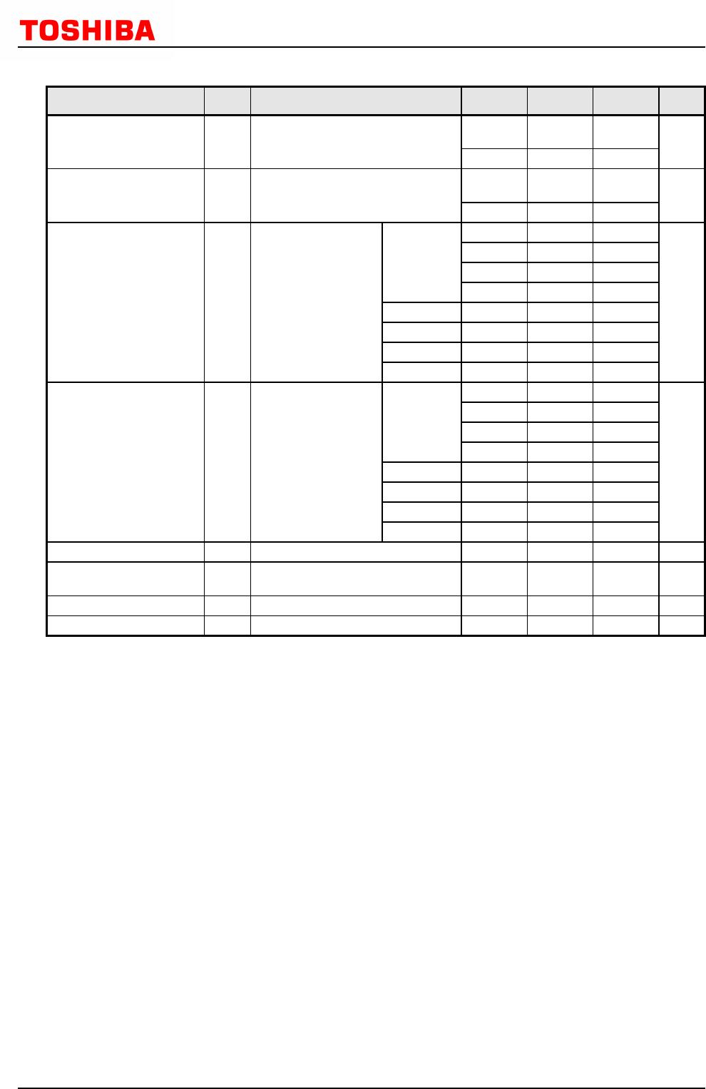
9.4. AC Characteristics (Unless otherwise specified, T
AC Characteristics (Unless otherwise specified, T
a
a
a
a
= 25
= 25
= 25
= 25
, Input: t
, Input: t
, Input: t
, Input: t
r
r
r
r
= t
= t
= t
= t
f
f
f
f
= 3 ns)
= 3 ns)
= 3 ns)
= 3 ns)
Characteristics
Propagation delay time
Output enable time
Output disable time
Input capacitance
Power dissipation
capacitance
Symbol
t
PLH
,t
PHL
t
PZL
,t
PZH
t
PLZ
,t
PHZ
C
IN
C
PD
Note
(Note 1)
Test Condition
R
L
= 1 M
See 9.7 AC Test
Circuit, Table 9.7.1
R
L
= 500
See 9.7 AC Test
Circuit, Table 9.7.1
R
L
= 500
See 9.7 AC Test
Circuit, Table 9.7.1
R
L
= 500
See 9.7 AC Test
Circuit, Table 9.7.1
V
CC
(V)
1.8 ± 0.15
2.5 ± 0.2
3.3 ± 0.3
5.0 ± 0.5
3.3 ± 0.3
5.0 ± 0.5
1.8 ± 0.15
2.5 ± 0.2
3.3 ± 0.3
5.0 ± 0.5
1.8 ± 0.15
2.5 ± 0.2
3.3 ± 0.3
5.0 ± 0.5
0 to 5.5
3.3
5.5
C
L
(pF)
15
50
50
50
Min
2.0
0.8
0.5
0.5
1.5
0.8
2.0
1.5
1.5
0.8
2.0
1.5
1.0
0.5
Typ.
5.3
3.4
2.5
2.1
3.2
2.6
7.0
4.6
3.5
2.8
5.4
3.5
2.8
2.1
4
17
24
Max
11.0
7.5
5.2
4.5
5.7
5.0
12.5
8.5
6.2
5.5
11.0
8.0
5.7
4.7
Unit
ns
ns
ns
ns
pF
pF
Note 1: C
PD
is defined as the value of the internal equivalent capacitance which is calculated from the operating current
consumption without load. Average operating current can be obtained by the equation.
I
CC(opr)
= C
PD
V
CC
f
IN
+ I
CC
9.5.
9.5.
9.5.
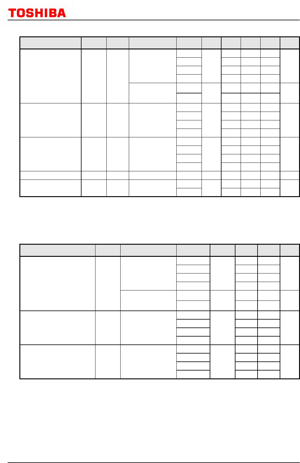
9.5. AC Characteristics
AC Characteristics
AC Characteristics
AC Characteristics
(Unless otherwise specified, T
a
a
a
a
= -40 to 85
= -40 to 85
= -40 to 85
= -40 to 85
, Input: t
, Input: t
, Input: t
, Input: t
r
r
r
r
= t
= t
= t
= t
f
f
f
f
= 3 ns)
= 3 ns)
= 3 ns)
= 3 ns)
Characteristics
Propagation delay time
Output enable time
Output disable time
Symbol
t
PLH
,t
PHL
t
PZL
,t
PZH
t
PLZ
,t
PHZ
Test Condition
R
L
= 1 M
See 9.7 AC Test Circuit,
Table 9.7.1
R
L
= 500
See 9.7 AC Test Circuit,
Table 9.7.1
R
L
= 500
See 9.7 AC Test Circuit,
Table 9.7.1
R
L
= 500
See 9.7 AC Test Circuit,
Table 9.7.1
V
CC
(V)
1.8 ± 0.15
2.5 ± 0.2
3.3 ± 0.3
5.0 ± 0.5
3.3 ± 0.3
5.0 ± 0.5
1.8 ± 0.15
2.5 ± 0.2
3.3 ± 0.3
5.0 ± 0.5
1.8 ± 0.15
2.5 ± 0.2
3.3 ± 0.3
5.0 ± 0.5
C
L
(pF)
15
50
50
50
Min
2.0
0.8
0.5
0.5
1.5
0.8
2.0
1.5
1.5
0.8
2.0
1.5
1.0
0.5
Max
11.5
8.0
5.5
4.8
6.0
5.3
13.0
9.0
6.5
5.8
12.0
8.5
6.0
5.0
Unit
ns
ns
ns
ns
2016-09-15
Rev.2.0
©2015 Toshiba Corporation

74LCX541MTCX

Mfr. #:
Manufacturer:
ON Semiconductor / Fairchild
Description:
Buffers & Line Drivers Octal Buff/Line Drv
Lifecycle:
New from this manufacturer.
Delivery:
DHL FedEx Ups TNT EMS
Payment:
T/T Paypal Visa MoneyGram Western Union

Products related to this Datasheet