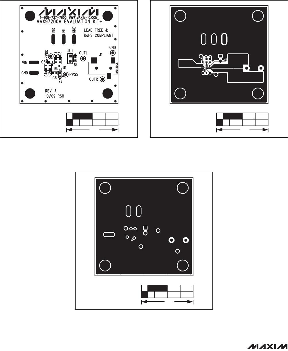
Figure 3. MAX97200A EV Kit PCB Layout—Component SideFigure 2. MAX97200A EV Kit Component Placement
Guide—Component Side
Figure 4. MAX97200A EV Kit PCB Layout—Layer 2
1.0”
1.0”
1.0”
Maxim cannot assume responsibility for use of any circuitry other than circuitry entirely embodied in a Maxim product. No circuit patent licenses are implied.
Maxim reserves the right to change the circuitry and specifications without notice at any time.
Maxim Integrated Products, 120 San Gabriel Drive, Sunnyvale, CA 94086 408-737-7600 5