LT6 020/LT6020-1
12
60201fa
For more information www.linear.com/LT6020
applicaTions inForMaTion
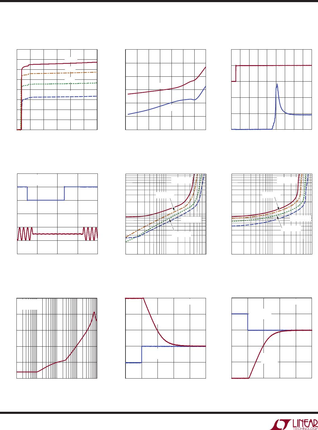
Figure 1. Settling Time Is Essentially Flat
smaller inputs the LT6020 slew rate approaches the slew
rate more common in traditional micropower amplifiers.
Input Bias Current
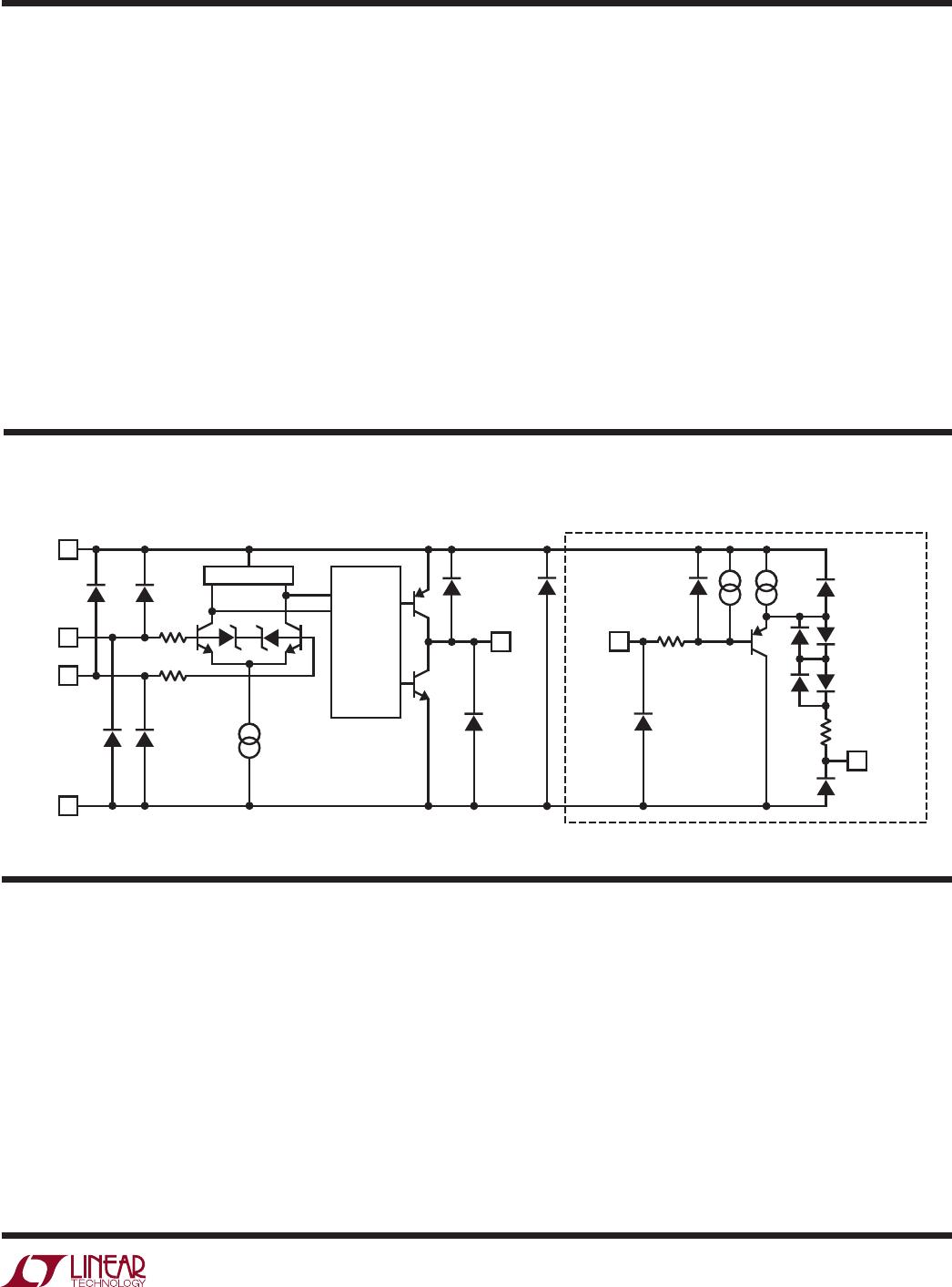
The design of the input stage of the LT6020 is more so
-
phisticated than that shown in the Simplified Schematic.
It
uses both NPN and PNP input differential amplifiers to
sense the input differential voltage. As a result the speci
-
fied input bias current can flow in or out of the input pins.
Multiplexer Applications/High Dynamic Input
Impedance
The LT6020 has features which make it desirable for
multiplexer applications, such as the application featured
on the back page of this data sheet. When the channels of
the multiplexer are cycled, the output of the multiplexer
can produce large voltage transitions. Normally, bipolar
amplifiers have back-to-back diodes between the inputs,
which will turn on when the input transient voltage exceeds
0.7V, causing a large transient current to be conducted
from the amplifier output stage back into the input driving
circuitry. The driving circuitry then needs to absorb this
current and settle before the amplifier can settle. The
LT6020 uses 5.5V Zener diodes to protect its inputs which
dramatically increases its
input impedance with input steps
as large as 5V.
Achieving Rail-to-Rail Operation without
Rail-to-Rail Inputs
The LT6020 output is able to swing close to each power
supply rail, but the input stage is limited to operating
between V
–
+ 1.2V and V
+
– 1.4V. For many inverting
applications and noninverting gain applications, this is
largely inconsequential. Figure 2 shows the basic op amp
configurations, what happens to the op amp inputs and
whether or not the op amp must have rail-to-rail inputs.
The circuit of Figure 3 shows an extreme example of the
inverting case. The input voltage at the 100k resistor can
swing ±13.5V and the LT6020 will output an inverted,
OUTPUT STEP (V
P-P
)
5
SETTLING TIME (µs)
30
25
20
15
10
5
0
20
60201 F01
2510 15
0.0015%
A
V
= 1
0.01%
The supply current of the LT6020 increases with large
differential input voltages. Normally, this does not impact
the low power nature of the LT6020 because the ampli
-
fier is forcing the two inputs to be at the same potential.
Conditions which cause differential input voltage to appear
should be avoided in order to preserve the low power dis
-
sipation of the LT6020. This includes but is not limited
to: operation as a comparator, excessive loading on the
output and overdriving the input.
Enhanced Slew Rate
The LT6020 uses a proprietary input stage which provides
an enhanced slew rate without sacrificing input precision
specs such as input offset voltage, common mode rejection
and noise. The unique input stage of the LT6020 allows the
output to quickly slew to its final value when large signal
input steps are applied. This enhanced slew characteristic
allows the LT6020 to quickly settle the output to 0.0015%
independent of input step size as shown in Figure 1. Typi
-
cal micropower amplifiers cannot process large amplitude
signals with this speed. As shown in the Typical Perfor-
mance cur
ves, when the LT6020 is configured in unity
gain
and a 10V step is applied to the input the output will
slew
at 5V/µs. In this same configuration, a 5V input step
will slew the output at 2.4V/µs. Furthermore, a 0.7V input
step will lower the slew rate to 0.2V/µs. Note that for these