LTC6087/LTC6088
9
60878fc
pin Functions
OUT: Amplifier Output.
–IN: Inverting Input.
+IN: Noninverting Input.
V
+
: Positive Supply.
V–: Negative Supply.
SHDNA: Shutdown Pin of Amplifier A, active low and only
available with the LTC 6087DD. An internal current source
pulls the pin to V
+
when floating.
SHDNB: Shutdown Pin of Amplifier B, active low and only
available with the LTC 6087DD. An internal current source
pulls the pin to V
+
when floating.
NC: Not internally connected
Exposed Pad: Connected to V
–
.
Rail-to-Rail Input
The input stage of LTC6087/LTC6088 combines both PMOS
and NMOS differential pairs, extending its input common
mode voltage to both positive and negative supply voltages.
At high input common mode range, the NMOS pair is on.
At low common mode range, the PMOS pair is on. The
transition happens when the common voltage is between
1.3V and 0.9V below the positive supply.
Achieving Low Input Bias Current
The DD and DHC packages are leadless and make contact
to the PCB beneath the package. Solder flux used during
the attachment of the part to the PCB can create leakage
current paths and can degrade the input bias current per-
formance
of the part. All inputs are susceptible because
the
backside paddle is connected to V
–
internally. As the
input voltage or V
–
changes, a leakage path can be formed
and alter the observed input bias current. For lowest bias
current use the LTC6087/LTC6088 in the leaded MSOP/
GN package. With fine PCB design rules, you can also
provide a guard ring around the inputs.
For example, in high source impedance applications such
as pH probes, photo diodes, strain gauges, et cetera, the
low input bias current of these parts requires a clean
board layout to minimize additional leakage current into a
high impedance signal node. A mere 100GΩ of PC board
resistance between a 5V supply trace and input trace near
ground potential adds 50pA of leakage current. This leak-
age is far greater than the bias current of the operational
amplifier. A guard ring around the high impedance input
traces driven by a low impedance source equal to the
input voltage prevents such leakage problems. The guard
ring should extend as far as necessary to shield the high
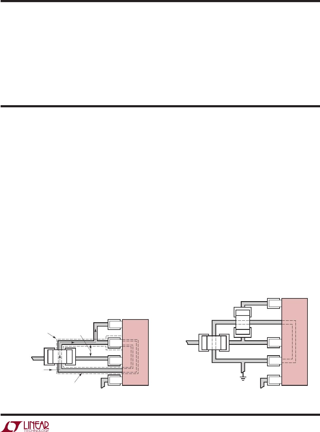
impedance signal from any and all leakage paths. Figure
1 shows the use of a guard ring in
a unity-gain configura-
tion.
In this case the guard ring is connected to the output
and is shielding the high impedance noninverting input
from V
–
. Figure 2 shows the inverting gain configuration.
Figure 1. Sample Layout. Unity-Gain Configuration. Using Guard
Ring to Shield High Impedance Input from Board Leakage
Figure 2. Sample Layout. Inverting Gain Configuration. Using
Guard Ring to Shield High Impedance Input from Board Leakage
applications inForMation
LTC6087
R
OUT
IN
–
IN
+
V
–
LEAKAGE
CURRENT
NO LEAKAGE
CURRENT
GUARD
RING
NO SOLDER MASK
OVER THE GUARD RING
60878 F01
LTC6087
60878 F02
R
R
OUT
IN
–
IN
+
V
–
V
IN
GND