MAX110/MAX111
Low-Cost, 2-Channel, ±14-Bit Serial ADCs
________________________________________________________________
Maxim Integrated Products
1
General Description
The MAX110/MAX111 analog-to-digital converters
(ADCs) use an internal auto-calibration technique to
achieve 14-bit resolution plus overrange, with no exter-
nal components. Operating supply current is only
550µA (MAX110) and reduces to 4µA in power-down
mode, making these ADCs ideal for high-resolution bat-
tery-powered or remote-sensing applications. A fast
serial interface simplifies signal routing and opto-isola-
tion, saves microcontroller pins, and offers compatibility
with SPI™, QSPI™, and MICROWIRE™. The MAX110
operates with ±5V supplies, and converts differential
analog signals in the -3V to +3V range. The MAX111
operates with a single +5V supply and converts differ-
ential analog signals in the ±1.5V range, or single-
ended signals in the 0V to +1.5V range.
Internal calibration allows for both offset and gain-error
correction under microprocessor (µP) control. Both
devices are available in space-saving 16-pin DIP and
SO packages, as well as an even smaller 20-pin SSOP
package.
________________________Applications
Process Control
Weigh Scales
Panel Meters
Data-Acquisition Systems
Temperature Measurement
____________________________Features
♦ Single +5V Supply (MAX111)
♦ Two Differential Input Channels
♦ 14-Bit Resolution Plus Sign and Overrange
♦ 0.03% Linearity (MAX110)
0.05% Linearity (MAX111)
♦ Low Power Consumption:
550µA (MAX110)
640µA (MAX111)
4µA Shutdown Current
♦ Up to 50 Conversions/sec
♦ 50Hz/60Hz Rejection
♦ Auto-Calibration Mode
♦ No External Components Required
♦ 16-Pin DIP/SO, 20-Pin SSOP
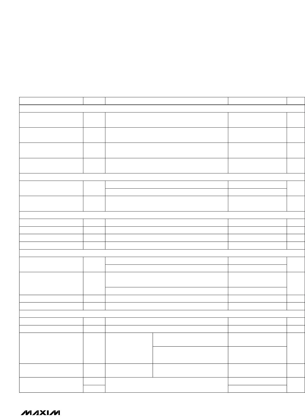
Ordering Information
19-0283; Rev 5; 11/98
Typical Operating Circuit
Pin Configurations
PART
MAX110ACPE
MAX110BCPE
MAX110ACWE 0°C to +70°C
0°C to +70°C
0°C to +70°C
TEMP. RANGE PIN-PACKAGE
16 Plastic DIP
16 Plastic DIP
16 Wide SO
MAX110BCWE 0°C to +70°C 16 Wide SO
MAX110ACAP 0°C to +70°C 20 SSOP
MAX110BCAP 0°C to +70°C 20 SSOP
EVALUATION KIT
AVAILABLE
MAX110BC/D 0°C to +70°C Dice*
Ordering Information continued at end of data sheet.
*
Contact factory for dice specifications.
SPI and QSPI are trademarks of Motorola, Inc. MICROWIRE is a trademark of National Semiconductor Corp.
Pin Configurations continued at end of data sheet.
INL(%)
±0.03
±0.05
±0.03
±0.05
±0.03
±0.05
±0.05
For free samples & the latest literature: http://www.maxim-ic.com, or phone 1-800-998-8800.
For small orders, phone 1-800-835-8769.