MAX110/MAX111
Low-Cost, 2-Channel, ±14-Bit Serial ADCs
______________________________________________________________________________________ 11
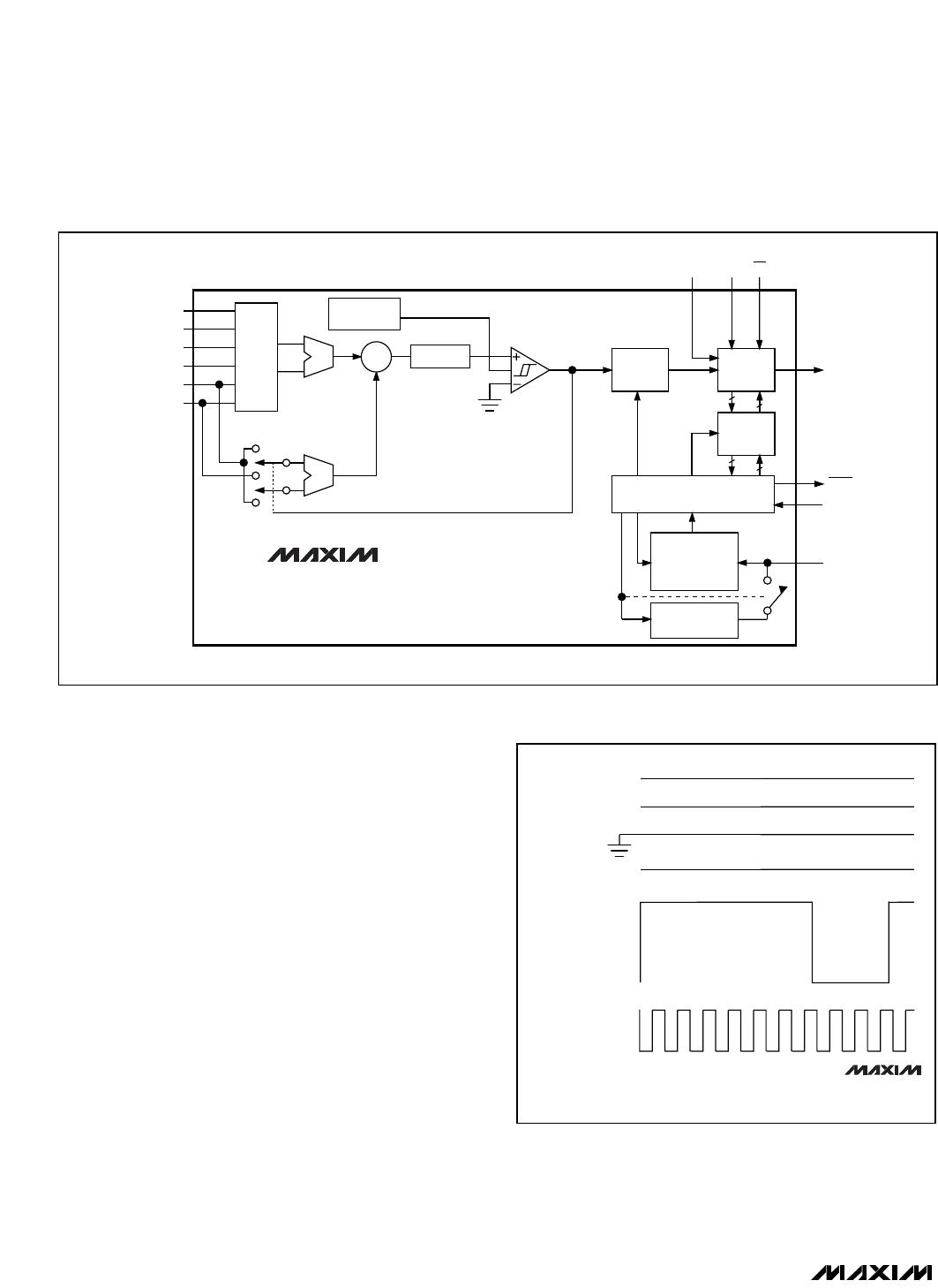
ADC Operation
The output data from the MAX110/MAX111 is arranged
in twos-complement format (Figures 4, 5). The sign bit
(POL) is shifted out first, followed by the overrange bit
(OR), and the 14 data bits (MSB first) (see Figure 6).
The MAX110 operates from ±5V power supplies and
converts low-frequency analog signals in the ±3V
range when using the maximum reference voltage of
V
REF
= 3V (V
REF
= V
REF+
- V
REF-
). Within the ±3V input
range, greater accuracy is obtained within ±2.5V (see
Electrical Characteristics
for details). Note that a nega-
tive input voltage is defined as V
IN-
> V
IN+
. For the
MAX110, the absolute voltage at any analog input pin
must remain within the (V
SS
+ 2.25V) to (V
DD
- 2.25V)
range.
The MAX111 operates from a single +5V supply and
converts low-frequency differential analog signals in the
±1.5V range when using the maximum reference volt-
age of V
REF
= 1.5V. As indicated in the
Electrical
Characteristics
, greater accuracy is achieved within the
±1.2V range. The absolute voltage at any analog input
pin for the MAX111 must remain within 0V to V
DD
- 3.2V.
When V
IN-
> V
IN+
the input is interpreted as negative.
The overrange bit (OFL) is provided to sense when the
input voltage level has exceeded the reference voltage
level. The converter does not “saturate” until the input
voltage is typically 20% larger. The linearity is not guar-
anteed in this range. Note that the overrange bit works
properly if the reference voltage remains within the rec-
ommended voltage range (see
Reference Inputs
). If the
reference voltage exceeds the recommended input
range, the overrange bit may not operate properly.
Digital Interface—Starting a Conversion
Data is transferred into and out of the serial I/O shift
register by pulling CS low and applying a serial clock
at SCLK. This fully static shift register allows SCLK to
range from DC to 2MHz. Output data from the ADC is
clocked out on SCLK’s falling edge and should be read
on SCLK’s rising edge. Input data to the ADC at DIN is
clocked in on SCLK’s rising edge. A new conversion
begins when CS returns high, provided the MSB in the
input control word (NO-OP) is a 1 (see
Using the
MAX110/MAX111 with MICROWIRE, SPI, and QSPI
Serial Interfaces
). Figure 6 shows the detailed serial-
interface timing diagram.
CCSS
must remain high during the conversion (while
BUSY remains low). Bringing CS low during the conver-
sion causes the ADC to stop converting, and may
result in erroneous output data.
Using the MAX110/MAX111 with SPI, QSPI, and
MICROWIRE Serial Interfaces
Figure 7 shows the most common serial-interface con-
nections. The MAX110/MAX111 are compatible with
SPI, QSPI (CPHA = 0, CPOL = 0), and MICROWIRE
serial-interface standards.