IRS2548D
www.irf.com © 2011 International Rectifie
5
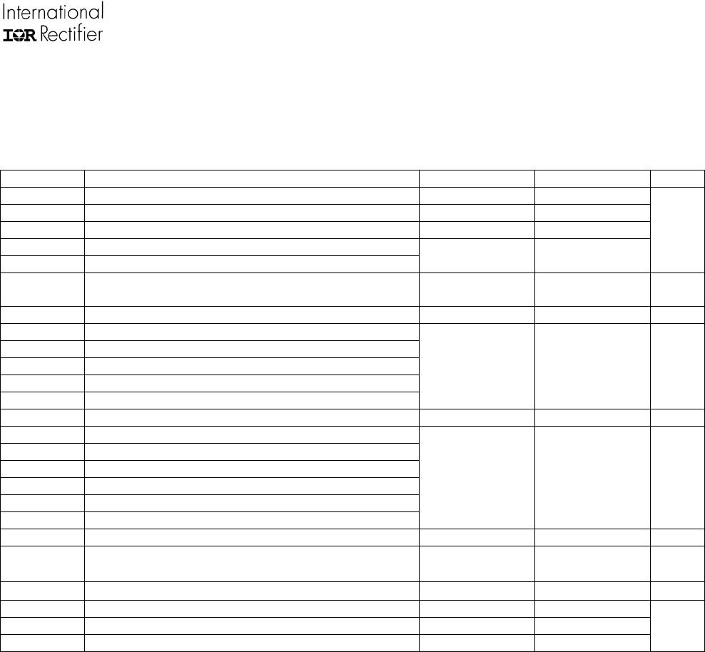
Absolute Maximum Ratings
Absolute maximum ratings indicate sustained limits beyond which damage to the device may occur. All
voltage parameters are absolute voltages referenced to COM, all currents are defined positive into any lead.
The thermal resistance and power dissipation ratings are measured under board mounted and still air
conditions.
Symbol Definition Min. Max. Units
V
B
VB Pin High-Side Floating Supply Voltage -0.3 625
V
S
VS Pin High-Side Floating Supply Offset Voltage
V
B
– 25 V
B
+ 0.3
V
HO
HO Pin High-Side Floating Output Voltage
V
S
- 0.3 V
B
+ 0.3
V
LO
LO Pin Low-Side Output Voltage
V
PFC
PFC Gate Driver Output Voltage
-0.3 V
CC
+ 0.3
V
IO
MAX
Maximum allowable output current (HO, LO, PFC)
due to external power transistor miller effect
-500 500 mA
ICC
VCC current
†
0 25 mA
V
VBUS
VBUS Pin Voltage
V
COMP
COMP Pin Voltage
VOC
OC Pin Voltage
V
ENN
SD/EOL Pin Voltage
V
CS
CS Pin Voltage
-0.3 V
CC
+ 0.3 V
VZX
ZX Pin Voltage
-0.3 VZX
CLAMP
+ 0.3 V
I
FMIN
FMIN Pin Current
I
COMP
COMP Pin Current
I
ZX
ZX Pin Current
I
OC
OC Pin Current
I
ENN
ENN Pin Current
I
CS
CS Pin Current
-5 5 mA
dV/dt Allowable VS Pin Offset Voltage Slew Rate -50 50 V/ns
P
D
Package Power Dissipation @ TA ≤ +25ºC
PD = (T
JMAX
-T
A
)/R
θJA
--- 1.0 W
R
θJA
Thermal Resistance, Junction to Ambient --- 120 ºC/W
T
J
Junction Temperature -55 150
T
S
Storage Temperature -55 150
T
L
Lead Temperature (soldering, 10 seconds) --- 300
ºC
†
This IC contains a zener clamp structure between the chip V
CC
and COM, with a nominal breakdown
voltage of 15.6 V. Please note that this supply pin should not be driven by a low impedance DC power source
greater than V
CLAMP
specified in the electrical characteristics section.

