IRS2548D
www.irf.com © 2011 International Rectifie
7
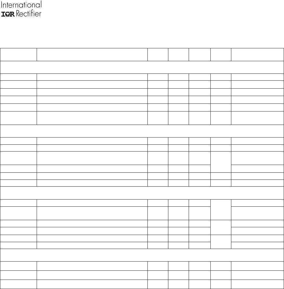
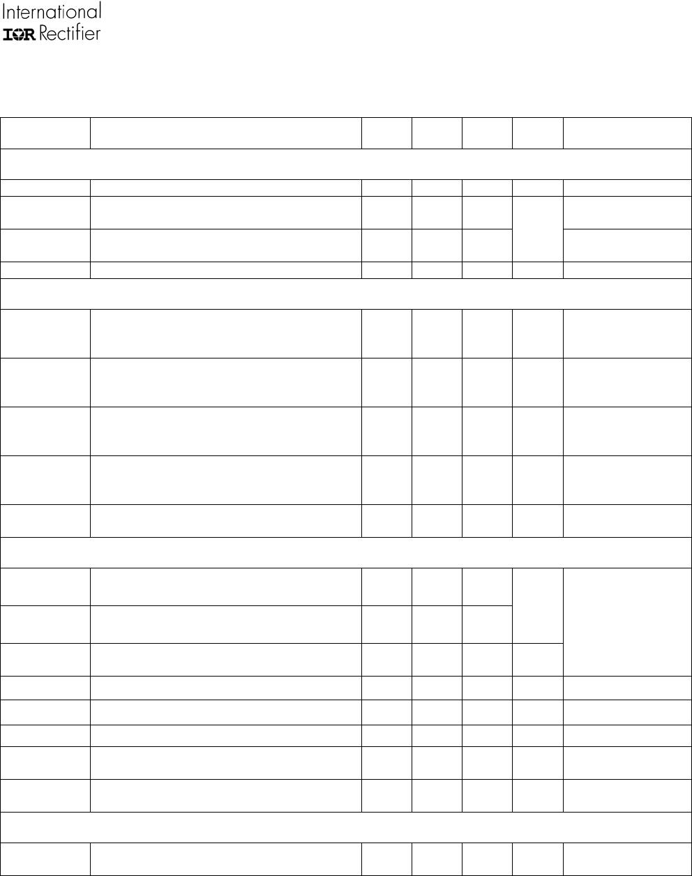
Electrical Characteristics (cont’d)
V
CC
= V
BS
= V
BIAS
=14V +/- 0.25V, C
LO
= C
HO
= C
PFC
= 1000pF, RFMIN = 42.2kOhm,
VENN
= V
COMP
= V
CS
= V
OC
= VBUS = VZX = 0V, T
A
=25C unless otherwise specified.
Symbol Definition Min Typ Max Units Test Conditions
Floating Supply Characteristics
I
BS
V
BS
Supply Current --- 0.9 1.3 mA MODE=RUN
V
BSUV+
V
BS
Supply Undervoltage Positive Going
Threshold
8.0 9.0 10.0
V
BS
rising from
0V
V
BSUV-
V
BS
Supply Undervoltage Negative
Going Threshold
7.0 8.0 9.0
V
V
BS
falling from
14V
I
LKVS
V
S
Offset Supply Leakage Current --- --- 50 uA V
B
= V
S
= 600V
PFC Error Amplifier Characteristics
I
COMP
SOURCE
COMP Pin OTA Error Amplifier Output
Current Sourcing
--- 30 --- uA
MODE = RUN
V
VBUS
= 3.5V
VCOMP=4.0V
I
COMP
SINK
COMP Pin OTA Error Amplifier Output
Current Sinking
--- -30 ---
MODE = RUN
V
VBUS
= 4.5V
VCOMP=4.0V
V
COMPOH
OTA Error Amplifier Output Voltage
Swing (high state)
--- 12.5 --- V
VBUS=3.5V
ICOMP=ICOMP_
SOURCE - 5uA
V
COMPOL
OTA Error Amplifier Output Voltage
Swing (low state)
--- 0.4 ---
VBUS=5.0V
ICOMP=ICOMP_
SINK + 5uA
VCOMPFLT
OTA Error Amplifier Output Voltage in
Fault Mode
--- 0 ---
VBUS=4.0V
PFC Control Characteristics
V
VBUS
REG
VBUS Internal Reference Voltage 3.93 4.03 4.13
V
VBUSOV
VBUS Over-voltage Comparator
Threshold
4.1 4.3 4.5
V
V
VBUSOV
HYS
VBUS Over-voltage Comparator
Hysteresis
50 150 300 mV
V
COMP
= 4.0V
V
ZX
ZX Pin Threshold Voltage 1.8 2.0 2.2 V
V
ZXhys
ZX pin Comparator Hysteresis --- 300 --- mV
V
ZXclamp
ZX pin Clamp Voltage (high state) --- 6.7 --- V I
ZX
= 1mA
t
BLANK
OC pin current-sensing blank time --- 300 --- ns
VBUS=4.0V
VCOMP=4.0V
t
WD
PFC Watch-dog Pulse Interval --- 400 --- us
ZX = 0, V
COMP
= 4.0V
PFC Protection Circuitry Characteristics
V
OCTH+
OC Pin Over-current Sense Threshold 1.1 1.2 1.3
VBUS=VCOMP
=4.0V