DOC#: SP-AP-0065 (Rev. AA) Page 9 of 22
Byte 14: Control Register 14
Table 4. Pin 6 and 7 Configuration Table
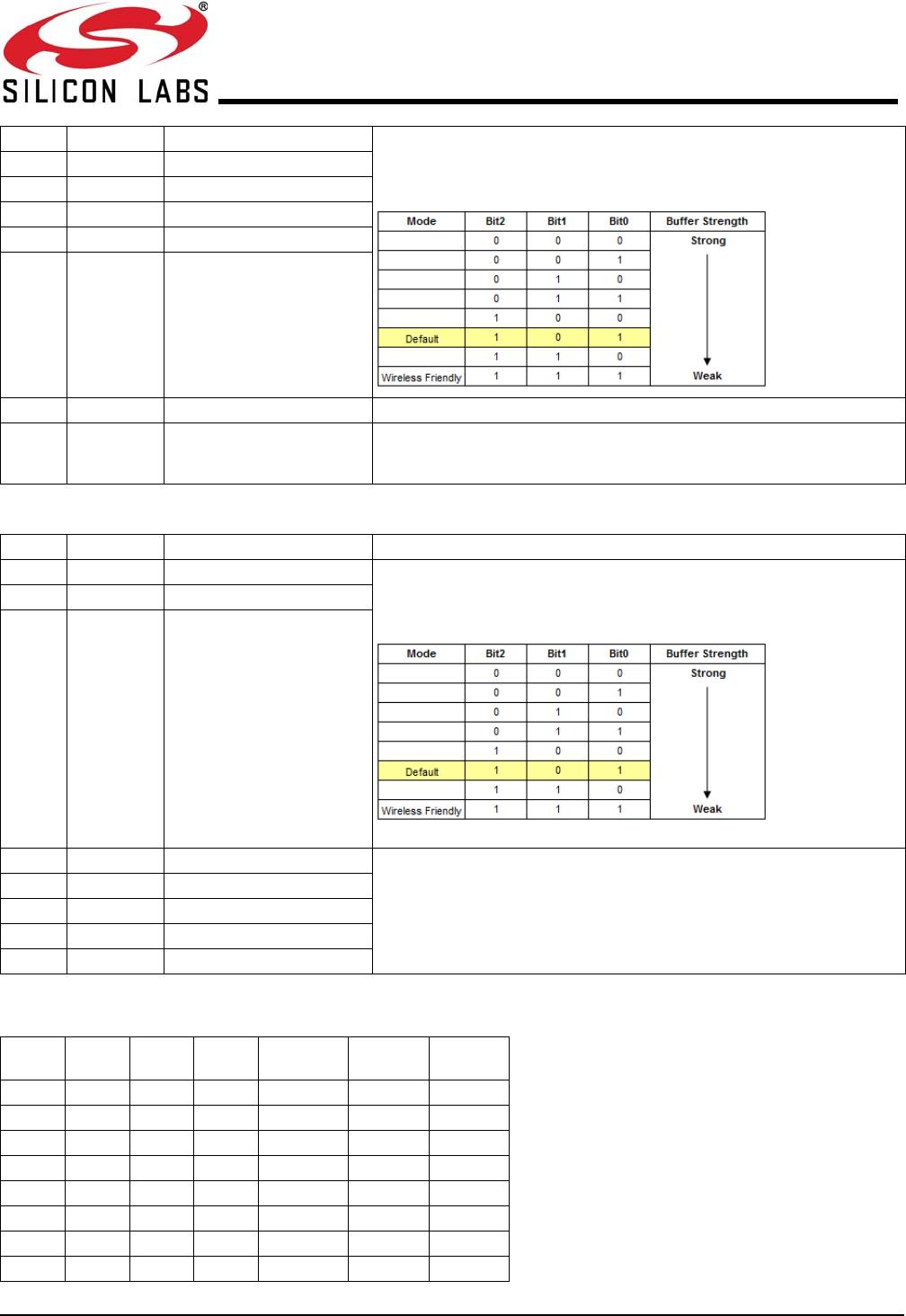
7 1 REF_Bit2 Drive Strength Control - Bit[2:0],
Note: See Byte 6 Bit 5 for REF Slew Rate Bit 1 and
Byte 6 Bit 3 for 27MHz Slew Rate Bit 1
Normal mode default ‘101’
Wireless Friendly Mode default to ‘111’
61 REF_Bit0
5 1 27MHz_NSS_Bit2
4 1 27MHz_NSS_Bit0
3 1 27MHz_SS_Bit2
2 1 27MHz_SS_Bit0
1 0 RESERVED RESERVED
0 0 Wireless Friendly mode Wireless Friendly Mode
0 = Disabled, Default all single-ended clocks slew rate config bits to ‘101’
1 = Enabled, Default all single-ended clocks slew rate config bits to ‘111’
Bit @Pup Name Description
7 1 USB_48_Bit2 Drive Strength Control - Bit[2:0] ,
Note: REF Bit 1is located in Byte 6 Bit 5 and 27MHz
Bit 1 is located in Byte 6 Bit 3
Normal mode default ‘101’
Wireless Friendly Mode default to ‘111’
6 0 USB_48_Bit1
5 1 USB_48_Bit0
40 OTP_4 OTP_ID
Identification for programmed device
30 OTP_3
20 OTP_2
10 OTP_1
00 OTP_0
B1b4 B1b3 B1b2 B1b1 Pin7 Pin 8 Spread
(%)
0000 N/A N/AN/A
0001 N/A N/AN/A
0 0 1 0 27M_NSS 27M_SS -0.5%
0 0 1 1 27M_NSS 27M_SS -1%
0 1 0 0 27M_NSS 27M_SS -1.5%
0 1 0 1 27M_NSS 27M_SS -2%
0 1 1 0 27M_NSS 27M_SS -0.75V
0 1 1 1 27M_NSS 27M_SS -1.25%

