3
0007N–PEEPR–9/09
AT28HC256
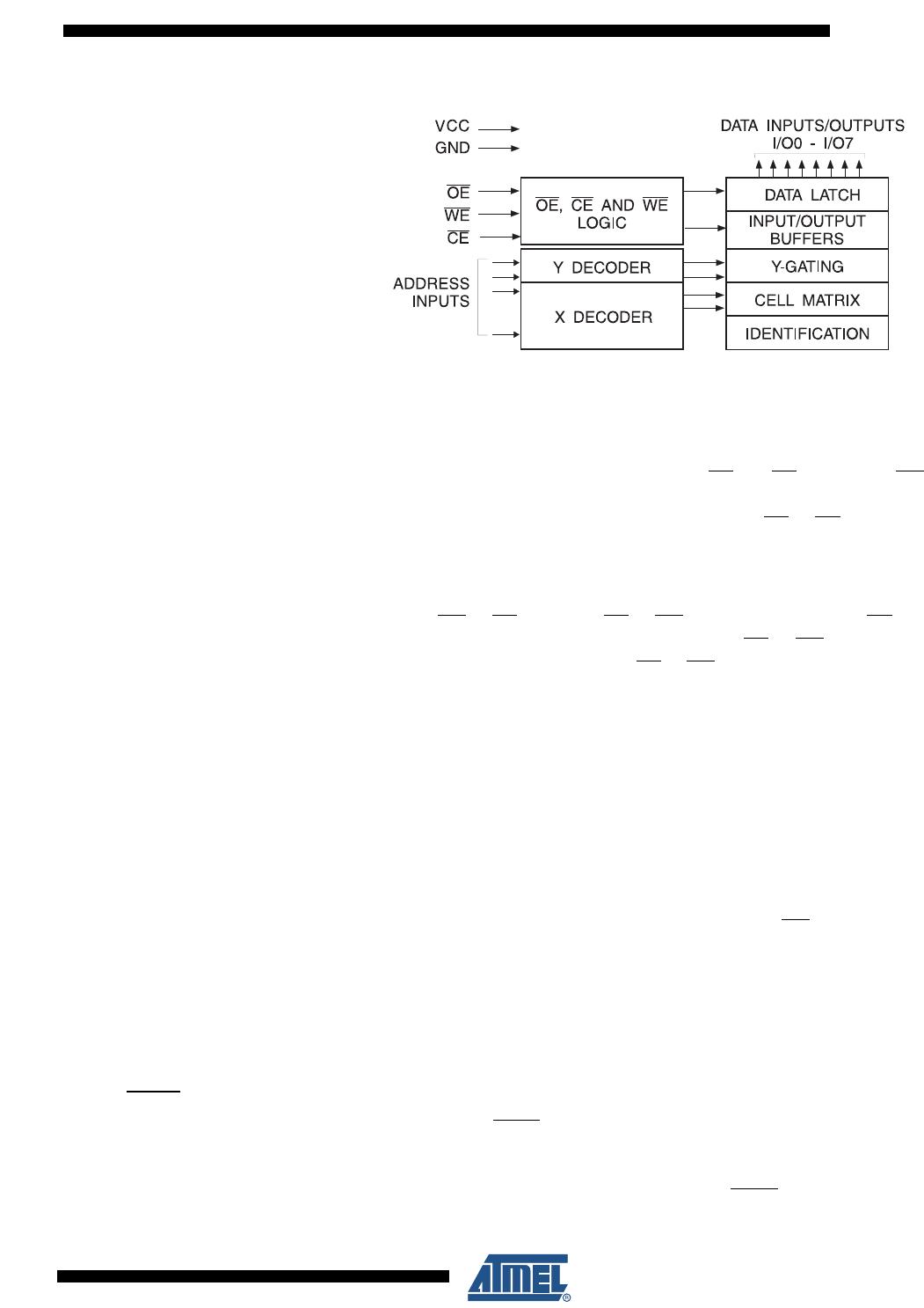
3. Block Diagram
4. Device Operation
4.1 Read
The AT28HC256 is accessed like a Static RAM. When CE and OE are low and WE is high, the
data stored at the memory location determined by the address pins is asserted on the outputs.
The outputs are put in the high impedance state when either CE
or OE is high. This dual-line
control gives designers flexibility in preventing bus contention in their system.
4.2 Byte Write
A low pulse on the WE or CE input with CE or WE low (respectively) and OE high initiates a
write cycle. The address is latched on the falling edge of CE
or WE, whichever occurs last.
The data is latched by the first rising edge of CE
or WE. Once a byte write has been started it
will automatically time itself to completion. Once a programming operation has been initiated
and for the duration of t
WC
, a read operation will effectively be a polling operation.
4.3 Page Write
The page write operation of the AT28HC256 allows 1 to 64 bytes of data to be written into the
device during a single internal programming period. A page write operation is initiated in the
same manner as a byte write; the first byte written can then be followed by 1 to 63 additional
bytes. Each successive byte must be written within 150 µs (t
BLC
) of the previous byte. If the
t
BLC
limit is exceeded the AT28C256 will cease accepting data and commence the internal
programming operation. All bytes during a page write operation must reside on the same page
as defined by the state of the A6 - A14 inputs. That is, for each WE
high to low transition dur-
ing the page write operation, A6 - A14 must be the same.
The A0 to A5 inputs are used to specify which bytes within the page are to be written. The
bytes may be loaded in any order and may be altered within the same load period. Only bytes
which are specified for writing will be written; unnecessary cycling of other bytes within the
page does not occur.
4.4 DATA Polling
The AT28HC256 features DATA Polling to indicate the end of a write cycle. During a byte or
page write cycle an attempted read of the last byte written will result in the complement of the
written data to be presented on I/O7. Once the write cycle has been completed, true data is
valid on all outputs, and the next write cycle may begin. DATA
Polling may begin at anytime
during the write cycle.