4
0007N–PEEPR–9/09
AT28HC256
4.5 Toggle Bit
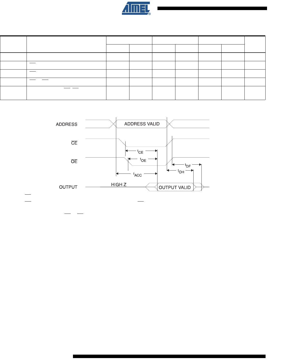
In addition to DATA Polling the AT28HC256 provides another method for determining the end
of a write cycle. During the write operation, successive attempts to read data from the device
will result in I/O6 toggling between one and zero. Once the write has completed, I/O6 will stop
toggling and valid data will be read. Testing the toggle bit may begin at any time during the
write cycle.
4.6 Data Protection
If precautions are not taken, inadvertent writes to any 5-volt-only nonvolatile memory may
occur during transition of the host system power supply. Atmel
®
has incorporated both hard-
ware and software features that will protect the memory against inadvertent writes.
4.6.1 Hardware Protection
Hardware features protect against inadvertent writes to the AT28HC256 in the following ways:
(a) V
CC
sense – if V
CC
is below 3.8V (typical) the write function is inhibited; (b) V
CC
power-on
delay – once V
CC
has reached 3.8V the device will automatically time out 5 ms typical) before
allowing a write; (c) write inhibit – holding any one of OE
low, CE high or WE high inhibits write
cycles; and (d) noise filter – pulses of less than 15 ns (typical) on the WE
or CE inputs will not
initiate a write cycle.
4.6.2 Software Data Protection
A software controlled data protection feature has been implemented on the AT28HC256.
When enabled, the software data protection (SDP), will prevent inadvertent writes. The SDP
feature may be enabled or disabled by the user; the AT28HC256 is shipped from Atmel with
SDP disabled.
SDP is enabled by the host system issuing a series of three write commands; three specific
bytes of data are written to three specific addresses (refer to “Software Data Protection” algo-
rithm). After writing the 3-byte command sequence and after t
WC
the entire AT28HC256 will be
protected against inadvertent write operations. It should be noted, that once protected the host
may still perform a byte or page write to the AT28HC256. This is done by preceding the data to
be written by the same 3-byte command sequence.
Once set, SDP will remain active unless the disable command sequence is issued. Power
transitions do not disable SDP and SDP will protect the AT28HC256 during power-up and
power-down conditions. All command sequences must conform to the page write timing spec-
ifications. It should also be noted that the data in the enable and disable command sequences
is not written to the device and the memory addresses used in the sequence may be written
with data in either a byte or page write operation.
After setting SDP, any attempt to write to the device without the three byte command
sequence will start the internal write timers. No data will be written to the device; however, for
the duration of t
WC
, read operations will effectively be polling operations.
4.7 Device Identification
An extra 64 bytes of EEPROM memory are available to the user for device identification. By
raising A9 to 12V ± 0.5V and using address locations 7FC0H to 7FFFH the additional bytes
may be written to or read from in the same manner as the regular memory array.
4.8 Optional Chip Erase Mode
The entire device can be erased using a 6-byte software code. Please see “Software Chip
Erase” application note for details.