Expand menu
Hello, Sign in
My Account
0
Cart
Home
Products
Sensors
Semiconductors
Passive Components
Connectors
Power
Electromechanical
Optoelectronics
Circuit Protection
Integrated Circuits - ICs
Main Products
Manufacturers
Blog
Services
About OMO
About Us
Contact Us
Check Stock
ZL40220LDG1
P1-P3
P4-P6
P7-P9
P10-P12
P13-P15
P16-P18
P19-P21
P22-P23
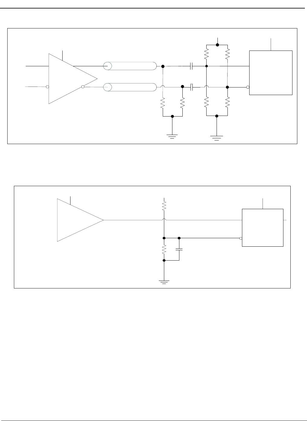
VDD
2 K
Ohm
VDD_dri
ver
VDD
ZL40220
clk_p
clk_n
Z
o
= 50 Ohms
Z
o
= 50 Ohms
2 K
Ohm
2 K
Ohm
2 K
Ohm
HCSL
Drive
r
100 nF
100 nF
50
Ohm
50
Ohm
Figure 10 - HCSL Input AC Coupled
VDD_dr
i
ver
VDD_dr
i
ver
VDD
ZL40220
cl
k_p
cl
k_n
CM
O
S
Dr
iv
er
R
R
C
Vref
= VDD_dri
ver
/2
R= 10 K ohm
s,
C = 100 nF
Figure 1
1 - CMOS Input DC Coupled Referenced to VDD/2
ZL40220
Data Sheet
10
Microsemi Corporation
VDD
VDD_driver
VDD
ZL40220
clk_p
clk_n
CMOS
Driver
R2
C
RA
R3
R1
Figure 12 - CMOS Input DC Coupled Reference
d to Ground
T
able 2 - Component V
alues for Single Ended Input Reference to Grou
nd
VDD_driver
R1 (k
Ω
)
R2 (k
Ω
)
R3 (k
Ω
)
RA (k
Ω
)
C (pF)
1.5
1.25
3.075
open
10
10
1.8
1
3.8
open
10
10
2.5
0.33
4.2
open
10
10
3.3
0.75
open
4.2
10
10
ZL40220
Data Sheet
11
Microsemi Corporation
* For frequencies below 100 MHz, incr
ease
C to avoid signal integrity issues.
ZL40220
Data Sheet
12
Microsemi Corporation
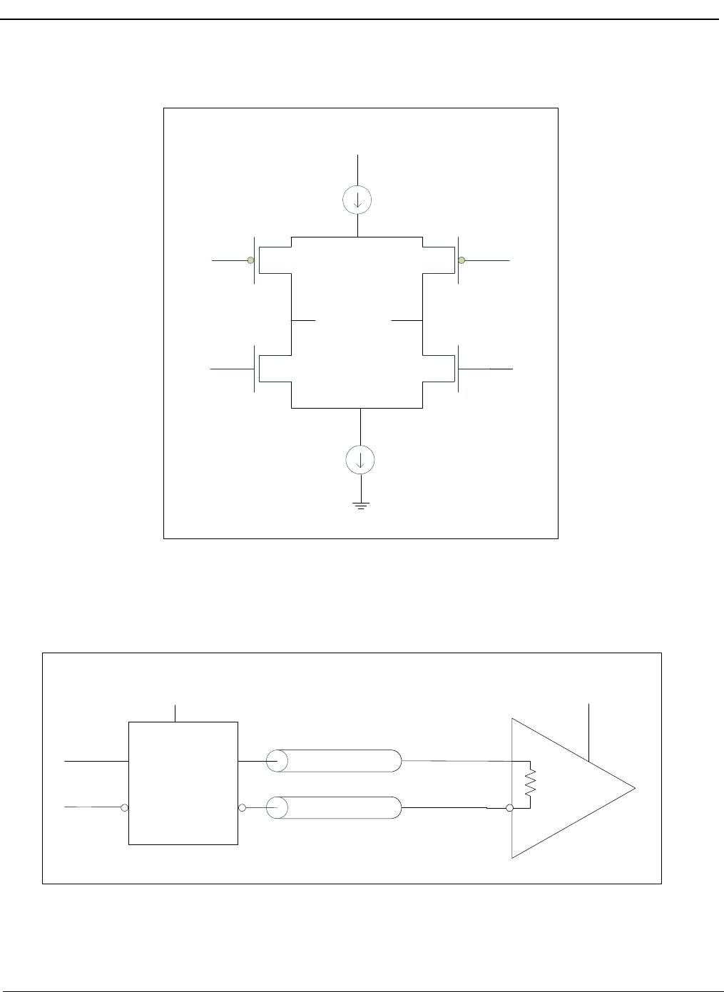
3.3 Clock Output
s
L
VDS has lower signal swing
than L
VPECL which results in
a low power consum
ption. A simplified diagram for the
L
VDS output sta
ge is shown in
Figure 13
.
VDD
3 mA
Output
-
+
+
-
Figure 13 - Simplified L
VDS Output Dr
iver
The methods to terminate the
ZL40220
drivers are shown in the follo
wing figures.
LVDS
Receiver
VDD
Z
o
= 50 Ohms
Z
o
= 50 Ohms
ZL40220
clk_p
clk_n
VDD_Rx
Figure 14 - L
VDS DC Coupled T
ermina
tion (Internal Receiver T
ermination)
P1-P3
P4-P6
P7-P9
P10-P12
P13-P15
P16-P18
P19-P21
P22-P23
ZL40220LDG1
Mfr. #:
Buy ZL40220LDG1
Manufacturer:
Microchip / Microsemi
Description:
Clock Buffer 2:6 LVDS Fanout Buffer w/Ext. Term.
Lifecycle:
New from this manufacturer.
Delivery:
DHL
FedEx
Ups
TNT
EMS
Payment:
T/T
Paypal
Visa
MoneyGram
Western
Union
Products related to this Datasheet
ZL40220LDG1
ZL40220LDF1