LT3791
13
3791fb
For more information www.linear.com/LT3791
operaTion
Buck Region (V
IN
> V
OUT
)
Switch M4 is always on and switch M3 is always off during
this mode. At the start of every cycle, synchronous switch
M2 is turned on first. Inductor current is sensed when
synchronous switch M2 is turned on. After the sensed
inductor current falls below the reference voltage, which
is proportional to V
C
, synchronous switch M2 is turned off
and switch M1 is turned on for the remainder of the cycle.
Switches M1 and M2 will alternate, behaving like a typical
synchronous buck regulator. The duty cycle of switch M1
increases until the maximum duty cycle of the converter
in buck operation reaches D
MAX(BUCK, TG1)
, given by:
D
MAX(BUCK,TG1)
= 100% – D
(BUCK-BOOST)
where D
(BUCK-BOOST)
is the duty cycle of the buck-boost
switch range:
D
(BUCK-BOOST)
= 8%
Figure 3 shows typical buck operation waveforms. If V
IN
approaches V
OUT
, the buck-boost region is reached.
Buck-Boost Region (V
IN
~ V
OUT
)
When V
IN
is close to V
OUT
, the controller is in buck-boost
operation. Figure 4 and Figure 5 show typical waveforms in
this operation. Every cycle the controller turns on switches
M2 and M4, then M
1 and M4 are turned on until 180° later
when switches M1 and M3 turn on, and then switches
M1 and M4 are turned on for the remainder of the cycle.
Figure 3. Buck Operation (V
IN
> V
OUT
)
M2 + M4 M2 + M4 M2 + M4
M1 + M4
3791 F03
M1 + M4M1 + M4
Figure 4. Buck-Boost Operation (V
IN
≤ V
OUT
)
Figure 5. Buck-Boost Operation (V
IN
≥ V
OUT
)
M2 + M4 M2 + M4 M2 + M4
M1 + M4M1 + M4M1 + M4
M1 + M4 M1 + M4 M1 + M4
M1+ M3 M1+ M3 M1+ M3
3791 F04
M2 + M4 M2 + M4 M2 + M4
M1 + M4 M1 + M4 M1 + M4
M1 + M3 M1 + M3 M1 + M3
3791 F05
LT3791
14
3791fb
For more information www.linear.com/LT3791
operaTion
Boost Region (V
IN
< V
OUT
)
Switch M1 is always on and synchronous switch M2 is
always off in boost operation. Every cycle switch M3 is
turned on first. Inductor current is sensed when synchro
-
nous switch M3 is turned on. After the sensed inductor
cur
rent exceeds the reference voltage which is proportional
to V
C
, switch M3 turns off and synchronous switch M4
is turned on for the remainder of the cycle. Switches M3
and M4 alternate, behaving like a typical synchronous
boost regulator.
The duty cycle of switch M3 decreases until the minimum
duty cycle of the converter in boost operation reaches
D
MIN(BOOST,BG2)
, given by:
D
MIN(BOOST,BG2)
= D
(BUCK-BOOST)
where D
(BUCK-BOOST)
is the duty cycle of the buck-boost
switch range:
D
(BUCK-BOOST)
= 8%
Figure 6 shows typical boost operation waveforms. If V
IN
approaches V
OUT
, the buck-boost region is reached.
M1 + M3
M1 + M3
M1 + M4
M1 + M4
M1 + M3
M1 + M4
3791 F06
Figure 6. Boost Operation (V
IN
< V
OUT
)
Low Current Operation
The LT3791 runs in forced continuous mode. In this mode
the controller behaves as a continuous, PWM current
mode synchronous switching regulator. In boost opera
-
tion, switch M1 is always on, switchM3 and synchronous
switch
M4 are alternately turned on to maintain the output
voltage independent of the direction of inductor current.
In buck operation, synchronous switch M4 is always on,
switch M1 and synchronous switch M2 are alternately
turned on to maintain the output voltage independent of
the direction of inductor current. In the forced continuous
mode, the output can source or sink current.
LT3791
15
3791fb
For more information www.linear.com/LT3791
applicaTions inForMaTion
The Typical Application on the front page is a basic LT3791
application circuit. External component selection is driven
by the load requirement, and begins with the selection of
R
SENSE
and the inductor value. Next, the power MOSFETs
are selected. Finally, C
IN
and C
OUT
are selected. This circuit
can operate up to an input voltage of 60V.
Programming The Switching Frequency
The RT frequency adjust pin allows the user to program the
switching frequency from 200kHz to 700kHz to optimize
efficiency/performance or external component size. Higher
frequency operation yields smaller component size but
increases switching losses and gate driving current, and
may not allow sufficiently high or low duty cycle operation.
Lower frequency operation gives better performance at the
cost of larger external component size. For an appropriate
R
T
resistor value see Table 1. An external resistor from
the RT pin to GND is required; do not leave this pin open.
Table 1. Switching Frequency vs R
T
Value
f
OSC
(kHz) R
T
(kΩ)
200 147
300 84.5
400 59.0
500 45.3
600 35.7
700 29.4
Frequency Synchronization
The LT3791 switching frequency can be synchronized
to an external clock using the SYNC pin. Driving SYNC
with a 50% duty cycle waveform is always a good choice,
otherwise maintain the duty cycle between 10% and 90%.
The rising edge of CLK_OUT corresponds to the rising edge
of SYNC thus allowing paralleling converters. The falling
edge of CLK_OUT turns on switch M3 and the rising edge
of CLK_OUT turns on switch M2.
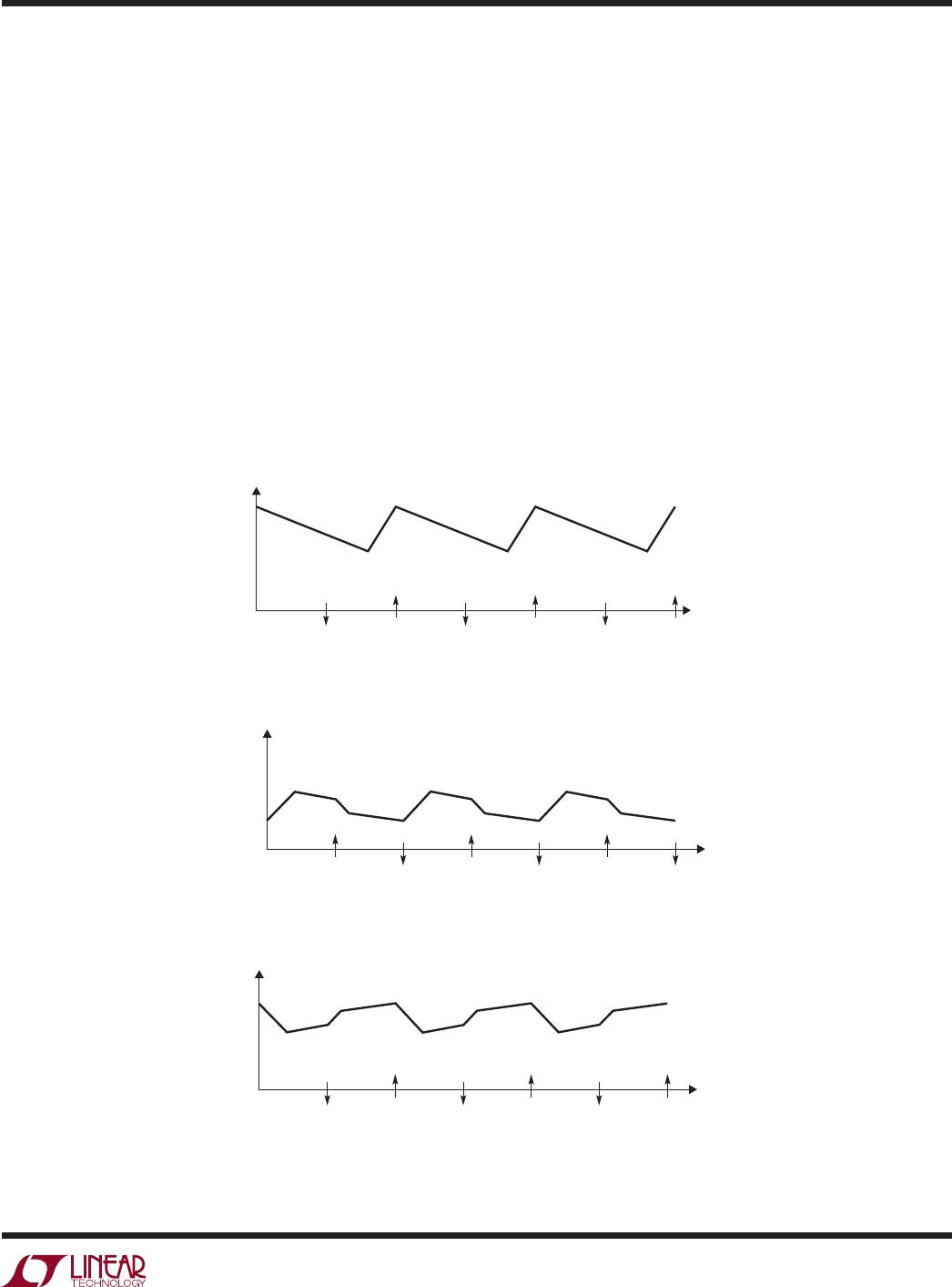
Inductor Selection
The operating frequency and inductor selection are inter
-
related in that higher operating frequencies allow the use
of
smaller inductor and capacitor values. The inductor
value has a direct effect on ripple current. The maximum
inductor current ripple ΔI
L
can be seen in Figure 7. This
is the maximum ripple that will prevent subharmonic
oscillation and also regulate with zero load. The ripple
should be less than this to allow proper operation over
all load currents. For a given ripple the inductance terms
in continuous mode are as follows:
L
BUCK
>
V
OUT
V
IN(MAX)
V
OUT
( )
100
f I
LED
%Ripple V
IN(MAX)
L
BOOST
>
V
IN(MIN)
2
V
OUT
V
IN(MIN)
( )
100
f I
LED
%Ripple V
OUT
2
where:
f is operating frequency
% ripple is allowable inductor current ripple
V
IN(MIN)
is minimum input voltage
V
IN(MAX)
is maximum input voltage
V
OUT
is output voltage
I
LED
is current through the LEDs

LT3791EFE#PBF

Mfr. #:
Manufacturer:
Analog Devices / Linear Technology
Description:
LED Lighting Drivers 60V 4-Switch Sync Buck-Boost LED Drvr Cn
Lifecycle:
New from this manufacturer.
Delivery:
DHL FedEx Ups TNT EMS
Payment:
T/T Paypal Visa MoneyGram Western Union