CAT24C256
www.onsemi.com
8
WRITE OPERATIONS
Byte Write
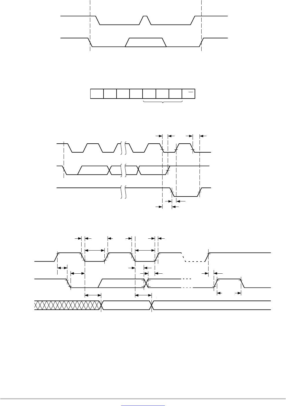
In Byte Write mode the Master sends a START, followed
by Slave address, two byte address and data to be written
(Figure 6). The Slave acknowledges all 4 bytes, and the
Master then follows up with a STOP, which in turn starts the
internal Write operation (Figure 7). During internal Write,
the Slave will not acknowledge any Read or Write request
from the Master.
Page Write
The CAT24C256 contains 32,768 bytes of data, arranged
in 512 pages of 64 bytes each. A two byte address word,
following the Slave address, points to the first byte to be
written. The most significant bit of the address word is ‘don’t
care’, the next 9 bits identify the page and the last 6 bits
identify the byte within the page. Up to 64 bytes can be
written in one Write cycle (Figure 8).
The internal byte address counter is automatically
incremented after each data byte is loaded. If the Master
transmits more than 64 data bytes, then earlier bytes will be
overwritten by later bytes in a ‘wrap−around’ fashion
(within the selected page). The internal Write cycle starts
immediately following the STOP.
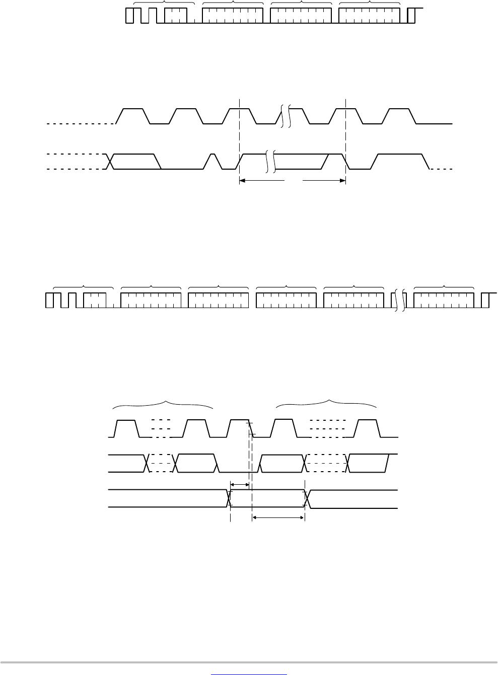
Acknowledge Polling
Acknowledge polling can be used to determine if the
CAT24C256 is busy writing or is ready to accept commands.
Polling is implemented by interrogating the device with a
‘Selective Read’ command (see READ OPERATIONS).
The CAT24C256 will not acknowledge the Slave address,
as long as internal Write is in progress.
Hardware Write Protection
With the WP pin held HIGH, the entire memory is
protected against Write operations. If the WP pin is left
floating or is grounded, it has no impact on the operation of
the CAT24C256. The state of the WP pin is strobed on the
last falling edge of SCL immediately preceding the first data
byte (Figure 9). If the WP pin is HIGH during the strobe
interval, the CAT24C256 will not acknowledge the data byte
and the Write request will be rejected.
Delivery State
The CAT24C256 is shipped erased, i.e., all bytes are FFh.