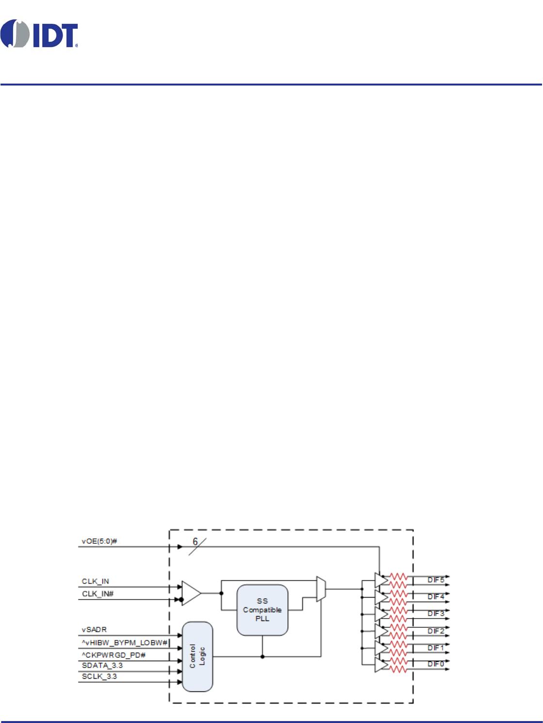
DATASHEET
9DBL0641 / 9DBL0651 FEBRUARY 8, 2017 1 ©2017 Integrated Device Technology, Inc.
6-output 3.3V PCIe Zero-Delay
Buffer
9DBL0641 / 9DBL0651
Description
The 9DBL0641 / 9DBL0651 devices are 3.3V members of
IDT's Full-Featured PCIe family. The 9DBL06 supports PCIe
Gen1-4 Common Clocked (CC) and PCIe Separate
Reference Independent Spread (SRIS) systems. It offers a
choice of integrated output terminations providing direct
connection to 85 or 100 transmission lines. The
9DBL06P1 can be factory programmed with a user-defined
power up default SMBus configuration.
Recommended Application
PCIe Gen1-4 clock distribution for Riser Cards, Storage,
Networking, JBOD, Communications, Access Points
Output Features
6 – 1-200 MHz Low-Power (LP) HCSL DIF pairs
9DBL0641 default ZOUT = 100
9DBL0651 default ZOUT = 85
9DBL06P1 factory programmable defaults
Key Specifications
PCIe Gen1-2-3-4 CC compliant in ZDB mode
PCIe Gen2 SRIS compliant in ZDB mode
Supports PCIe Gen2-3 SRIS in fan-out mode
DIF cycle-to-cycle jitter <50ps
DIF output-to-output skew < 50ps
Bypass mode additive phase jitter is 0 ps typical rms for
PCIe
Bypass mode additive phase jitter 160fs rms typ. @
156.25M (1.5M to 10M)
Features/Benefits
Direct connection to 100 (xx41) or 85 (xx51)
transmission lines; saves 24 resistors compared to
standard PCIe devices
149mW typical power consumption (PLL mode@3.3V);
eliminates thermal concerns
VDDIO allows 30% power savings at optional 1.05V;
maximum power savings
SMBus-selectable features allows optimization to customer
requirements:
control input polarity
control input pull up/downs
slew rate for each output
differential output amplitude
output impedance for each output
50, 100, 125MHz operating frequency
Customer defined SMBus power up default can be
programmed into P1 device; allows exact optimization to
customer requirements
OE# pins; support DIF power management
HCSL-compatible differential input; can be driven by
common clock sources
Spread Spectrum tolerant; allows reduction of EMI
Pin/SMBus selectable PLL bandwidth and PLL Bypass;
minimize phase jitter for each application
Outputs blocked until PLL is locked; clean system start-up
Device contains default configuration; SMBus interface not
required for device operation
Three selectable SMBus addresses; multiple devices can
easily share an SMBus segment
Space saving 40-pin 5x5mm VFQFPN; minimal board
space
Block Diagram
Note: Default resistors are internal on xx41/xx51 devices. P1 devices have programmable default impedances on an output-by-output basis.
6-OUTPUT 3.3V PCIE ZERO-DELAY BUFFER 2 FEBRUARY 8, 2017
9DBL0641 / 9DBL0651 DATASHEET
Pin Configuration
SMBus Address Selection Table
Power Management Table
Power Connections PLL Operating Mode
^CKPWRGD_PD#
VDDIO
vOE5#
DIF5#
DIF5
vOE4#
DIF4#
DIF4
VDDIO
VDD3.3
40 39 38 37 36 35 34 33 32 31
vSADR_tri
130
NC
^vHIBW_BYPM_LOBW#
229
vOE3#
FB_DNC
328
DIF3#
FB_DNC#
427
DIF3
VDDR3.3
526
VDDIO
CLK_IN
625
VDDA3.3
CLK_IN#
724
vOE2#
GNDDIG
823
DIF2#
SCLK_3.3
922
DIF2
SDATA_3.3
10 21
vOE1#
11 12 13 14 15 16 17 18 19 20
VDDDIG3.3
VDDIO
vOE0#
DIF0
DIF0#
VDD3.3
VDDIO
DIF1
DIF1#
NC
9DBL0641/51/P1
epad is GND
40-VFQFPN, 5mm x 5mm 0.4mm pin pitch
^ prefix indicates internal 120KOhm pull up resistor
^v prefix indicates internal 120KOhm pull up AND pull down resistor (biased to VDD/2)
v prefix indicates internal 120KOhm pull down resistor
SADR Address
0 1101011
M 1101100
1 1101101
x
x
State of SADR on first application of
CKPWRGD_PD#
+ Read/Write bit
x
Note: If not using CKPWRGD (CKPWRGD tied to VDD3.3), all 3.3V VDD need to transition
from 2.1V to 3.135V in <300usec.
True O/P Comp. O/P
0XXX
Low
1
Low
1
Off
1 Running 0 X
Low
1
Low
1
On
2
1 Running 1 0 Running Running
On
2
1 Running 1 1
Low
1
Low
1
On
2
1. The output state is set by B11[1:0] (Low/Low default)
PLL
2. If Bypass mode is selected, the PLL will be off, and outputs will be running.
CKPWRGD_PD# CLK_IN
SMBus
OEx bit
OEx# Pin
DIFx
Pin Number
VDD VDDIO GND
541
Input
receiver
analo
g
11 8 Digital Power
16, 31
12,17,26,32,
39
41
DIF outputs,
Lo
g
ic
25 41 PLL Analog
Description
HiBW_BypM_LoBW# MODE
Byte1 [7:6]
Readback
Byte1 [4:3]
Control
0 PLL Lo BW 00 00
MBypass0101
1 PLL Hi BW 11 11
FEBRUARY 8, 2017 3 6-OUTPUT 3.3V PCIE ZERO-DELAY BUFFER
9DBL0641 / 9DBL0651 DATASHEET
Pin Descriptions
PIN # PIN NAME PIN TYPE DESCRIPTION
1 vSADR_tri
LATCHED
IN
Tri-level latch to select SMBus Address. See SMBus Address Selection Table.
2 ^vHIBW_BYPM_LOBW#
LATCHED
IN
Trilevel input to select High BW, Bypass or Low BW mode. This pin is biased to VDD/2 (Bypass
mode) with internal pull up/pull down resistors. See PLL Operating Mode Table for Details.
3 FB_DNC DNC
True clock of differential feedback. The feedback output and feedback input are connected
internally on this pin. Do not connect anything to this pin.
4 FB_DNC# DNC
Complement clock of differential feedback. The feedback output and feedback input are
connected internally on this pin. Do not connect anything to this pin.
5 VDDR3.3 PWR
3.3V power for differential input clock (receiver). This VDD should be treated as an Analog
power rail and filtered appropriately.
6 CLK_IN IN True Input for differential reference clock.
7 CLK_IN# IN Complementary Input for differential reference clock.
8 GNDDIG GND Ground pin for digital circuitry
9 SCLK_3.3 IN Clock pin of SMBus circuitry, 3.3V tolerant.
10 SDATA_3.3 I/O Data pin for SMBus circuitry, 3.3V tolerant.
11 VDDDIG3.3 PWR 3.3V digital power (dirty power)
12 VDDIO PWR Power supply for differential outputs
13 vOE0# IN
Active low input for enabling DIF pair 0. This pin has an internal pull-down.
1 =disable outputs, 0 = enable outputs
14 DIF0 OUT Differential true clock output
15 DIF0# OUT Differential Complementary clock output
16 VDD3.3 PWR Power supply, nominal 3.3V
17 VDDIO PWR Power supply for differential outputs
18 DIF1 OUT Differential true clock output
19 DIF1# OUT Differential Complementary clock output
20 NC N/A No Connection.
21 vOE1# IN
Active low input for enabling DIF pair 1. This pin has an internal pull-down.
1 =disable outputs, 0 = enable outputs
22 DIF2 OUT Differential true clock output
23 DIF2# OUT Differential Complementary clock output
24 vOE2# IN
Active low input for enabling DIF pair 2. This pin has an internal pull-down.
1 =disable outputs, 0 = enable outputs
25 VDDA3.3 PWR 3.3V power for the PLL core.
26 VDDIO PWR Power supply for differential outputs
27 DIF3 OUT Differential true clock output
28 DIF3# OUT Differential Complementary clock output
29 vOE3# IN
Active low input for enabling DIF pair 3. This pin has an internal pull-down.
1 =disable outputs, 0 = enable outputs
30 NC N/A No Connection.
31 VDD3.3 PWR Power supply, nominal 3.3V
32 VDDIO PWR Power supply for differential outputs
33 DIF4 OUT Differential true clock output
34 DIF4# OUT Differential Complementary clock output
35 vOE4# IN
Active low input for enabling DIF pair 4. This pin has an internal pull-down.
1 =disable outputs, 0 = enable outputs
36 DIF5 OUT Differential true clock output
37 DIF5# OUT Differential Complementary clock output
38 vOE5# IN
Active low input for enabling DIF pair 5. This pin has an internal pull-down.
1 =disable outputs, 0 = enable outputs
39 VDDIO PWR Power supply for differential outputs
40 ^CKPWRGD_PD# IN
Input notifies device to sample latched inputs and start up on first high assertion. Low enters
Power Down Mode, subsequent high assertions exit Power Down Mode. This pin has internal
pull-up resistor.
41 ePAD GND Connect paddle to ground.

9DBL0651BKILF

Mfr. #:
Manufacturer:
IDT
Description:
Clock Buffer 3.3V LP-HCSL PCIE ZDB FOB
Lifecycle:
New from this manufacturer.
Delivery:
DHL FedEx Ups TNT EMS
Payment:
T/T Paypal Visa MoneyGram Western Union

Products related to this Datasheet