AD7401A
Rev. C | Page 12 of 20
8
–8
–0.35
0.35
V
IN
– DC INPUT (V)
I
IN
(µA)
6
4
2
0
–2
–4
–6
–0.30
–0.25
–0.20
–0.15
–0.10
–0.05
0
0.05
0.10
0.15
0.20
0.25
0.30
V
DD1
= V
DD2
= 4.5V TO 5.25V
MCLKIN = 10MHz
MCLKIN = 5MHz
MCLKIN = 16MHz
07332-018
Figure 18. I
IN
vs. V
IN
− DC Input
0
–120
0.1 1000
RIPPLE FREQUENCY (kHz)
CMRR (dB)
–20
–40
–60
–80
–100
1 10 100
V
DD1
= V
DD2
= 5 V
V
DD1
= V
DD2
= 5V
MCLKIN = 16MHz
MCLKIN = 5MHz
MCLKIN = 10MHz
07332-019
Figure 19. CMRR vs. Common-Mode Ripple Frequency
1.0
0
V
IN
DC INPUT (V)
NOISE (mV)
0.8
0.6
0.4
0.2
V
DD1
= V
DD2
= 5V
50kHz BRICK-WALL FILTER
MCLKIN = 5MHz
MCLKIN = 10MHz
MCLKIN = 16MHz
07332-020
–0.30
–0.25
–0.20
–0.15
–0.10
–0.05
0
0.05
0.10
0.15
0.20
0.25
0.30
Figure 20. RMS Noise Voltage vs. V
IN
DC Input
AD7401A
Rev. C | Page 13 of 20
TERMINOLOGY
Differential Nonlinearity (DNL)
DNL is the difference between the measured and the ideal 1
LSB change between any two adjacent codes
in the ADC.
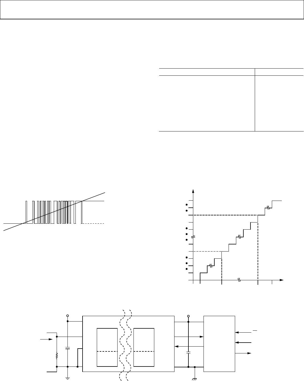
Integral Nonlinearity (INL)
INL is the maximum deviation from a straight line passing
through the endpoints of the ADC transfer function. The
endpoints of the transfer function are specified negative full
scale, −250 mV (V
IN
+ − V
IN
−), Code 7169 for the 16-bit level,
and specified positive full scale, +250 mV (V
IN
+ − V
IN
−), Code
58366 for the 16-bit level.
Offset Error
Offset error is the deviation of the midscale code (32768 for the
16-bit level) from the ideal V
IN
+ − V
IN
− (that is, 0 V).
Gain Error
The gain error includes both positive full-scale gain error and
negative full-scale gain error. Positive full-scale gain error is the
deviation of the specified positive full-scale code (58366 for the
16-bit level) from the ideal V
IN
+ − V
IN
− (+250 mV) after the
offset error is adjusted out. Negative full-scale gain error is the
deviation of the specified negative full-scale code (7169 for the
16-bit level) from the ideal V
IN
+ − V
IN
− (−250 mV) after the
offset error is adjusted out. Gain error includes reference error.
Signal-to-(Noise and Distortion) Ratio (SINAD)
SINAD is the measured ratio of signal-to-noise and distortion
at the output of the ADC. The signal is the rms amplitude of the
fundamental. Noise is the sum of all nonfundamental signals up
to half the sampling frequency (f
S
/2), excluding dc. The ratio is
dependent on the number of quantization levels in the digitization
process; the more levels, the smaller the quantization noise. The
theoretical signal-to-(noise and distortion) ratio for an ideal
N-bit converter with a sine wave input is given by
Signal-to-(Noise and Distortion) = (6.02N + 1.76) dB
Therefore, for a 12-bit converter, this is 74 dB.
Effective Number of Bits (ENOB)
ENOB is defined by
ENOB = (SINAD − 1.76)/6.02 bits
Total Harmonic Distortion (THD)
THD is the ratio of the rms sum of harmonics to the
fundamental. For the AD7401A, it is defined as
1
6
54
32
V
VVVVV
THD
22222
log20(dB)
++++
=
where:
V
1
is the rms amplitude of the fundamental.
V
2
, V
3
, V
4
, V
5
, and V
6
are the rms amplitudes of the second
through the sixth harmonics.
Peak Harmonic or Spurious Noise
Peak harmonic or spurious noise is defined as the ratio of the
rms value of the next largest component in the ADC output
spectrum (up to f
S
/2, excluding dc) to the rms value of the
fundamental. Normally, the value of this specification is
determined by the largest harmonic in the spectrum, but
for ADCs where the harmonics are buried in the noise floor,
it is a noise peak.
Common-Mode Rejection Ratio (CMRR)
CMRR is defined as the ratio of the power in the ADC output
at ±250 mV frequency, f, to the power of a 250 mV p-p sine
wave applied to the common-mode voltage of V
IN
+ and V
IN
of frequency, f
S
, as
CMRR (dB) = 10 .log(Pf/Pf
S
)
where:
Pf is the power at frequency, f, in the ADC output.
Pf
S
is the power at frequency, f
S
, in the ADC output.
Power Supply Rejection Ratio (PSRR)
Variations in power supply affect the full-scale transition but
not the converter’s linearity. PSRR is the maximum change in
the specified full-scale (±250 mV) transition point due to a
change in power supply voltage from the nominal value (see
Figure 6).
Isolation Transient Immunity
The isolation transient immunity specifies the rate of rise/fall of
a transient pulse applied across the isolation boundary beyond
which clock or data is corrupted. The AD7401A was tested
using a transient pulse frequency of 100 kHz.
AD7401A
Rev. C | Page 14 of 20
THEORY OF OPERATION
CIRCUIT INFORMATION
The AD7401A isolated Σ-Δ modulator converts an analog input
signal into a high speed (20 MHz maximum), single-bit data
stream; the time average single-bit data from the modulators
is directly proportional to the input signal. Figure 23 shows a
typical application circuit where the AD7401A is used to provide
isolation between the analog input, a current sensing resistor,
and the digital output, which is then processed by a digital filter
to provide an N-bit word.
ANALOG INPUT
The differential analog input of the AD7401A is implemented
with a switched capacitor circuit. This circuit implements a
second-order modulator stage that digitizes the input signal
into a 1-bit output stream. The sample clock (MCLKIN)
provides the clock signal for the conversion process as well as
the output data-framing clock. This clock source is external
on the AD7401A. The analog input signal is continuously
sampled by the modulator and compared to an internal
voltage reference. A digital stream that accurately represents
the analog input over time appears at the output of the
converter (see Figure 21).
MODULATOR OUTPUT
+FS ANALOG INPUT
–FS ANALOG INPUT
ANALOG INPUT
07332-021
Figure 21. Analog Input vs. Modulator Output
A differential signal of 0 V results (ideally) in a stream of alter-
nating 1s and 0s at the MDAT output pin. This output is high
50% of the time and low 50% of the time. A differential input of
200 mV produces a stream of 1s and 0s that are high 81.25% of
the time (for a +250 mV input, the output stream is high 89.06% of
the time). A differential input of −200 mV produces a stream of
1s and 0s that are high 18.75% of the time (for a −250 mV
input, the output stream is high 10.94% of the time).
A differential input of 320 mV results in a stream of, ideally, all
1s. This is the absolute full-scale range of the AD7401A, and
200 mV is the specified full-scale range, as shown in Table 9.
Table 9. Analog Input Range
Analog Input Voltage Input
Full-Scale Range +640 mV
Positive Full Scale +320 mV
Positive Typical Input Range +250 mV
Positive Specified Input Range +200 mV
Zero 0 mV
Negative Specified Input Range −200 mV
Negative Typical Input Range −250 mV
Negative Full Scale −320 mV
To reconstruct the original information, this output needs to be
digitally filtered and decimated. A sinc3 filter is recommended
because this is one order higher than that of the AD7401A modu-
lator. If a 256 decimation rate is used, the resulting 16-bit word
rate is 62.5 kHz, assuming a 16 MHz external clock frequency.
Figure 22 shows the transfer function of the AD7401A relative
to the 16-bit output.
65535
53248
SPECIFIED RANGE
ANALOG INPUT
ADC CODE
12288
–320mV –200mV +200mV +320mV
0
07332-022
Figure 22. Filtered and Decimated 16-Bit Transfer Characteristic
Σ-
MOD/
ENCODER
INPUT
CURRENT
NONISOL
A
TED
5V/3V
ISO
L
A
TED
5V
V
DD1
R
SHUNT
V
IN
+
V
IN
GND
1
V
DD
GND
V
DD2
MDAT MDAT
SINC3 FILTER*
AD7401A
MCLKIN
SDAT
CS
SCLK
MCLK
GND
2
DECODER
DECODER
+
ENCODER
07332-023
*THIS FILTER IS IMPLEMENTED
WITH AN FPGA OR DSP.
Figure 23. Typical Application Circuit

AD7401AYRWZ

Mfr. #:
Manufacturer:
Analog Devices Inc.
Description:
Analog to Digital Converters - ADC Isolated Modulator
Lifecycle:
New from this manufacturer.
Delivery:
DHL FedEx Ups TNT EMS
Payment:
T/T Paypal Visa MoneyGram Western Union

Products related to this Datasheet