© Semiconductor Components Industries, LLC, 2016
October, 2016 − Rev. 29
1 Publication Order Number:
LM324/D
LM324, LM324A, LM324E,
LM224, LM2902, LM2902E,
LM2902V, NCV2902
Single Supply Quad
Operational Amplifiers
The LM324 series are low−cost, quad operational amplifiers with
true differential inputs. They have several distinct advantages over
standard operational amplifier types in single supply applications. The
quad amplifier can operate at supply voltages as low as 3.0 V or as
high as 32 V with quiescent currents about one−fifth of those
associated with the MC1741 (on a per amplifier basis). The common
mode input range includes the negative supply, thereby eliminating the
necessity for external biasing components in many applications. The
output voltage range also includes the negative power supply voltage.
Features
• Short Circuited Protected Outputs
• True Differential Input Stage
• Single Supply Operation: 3.0 V to 32 V
• Low Input Bias Currents: 100 nA Maximum (LM324A)
• Four Amplifiers Per Package
• Internally Compensated
• Common Mode Range Extends to Negative Supply
• Industry Standard Pinouts
• ESD Clamps on the Inputs Increase Ruggedness without Affecting
Device Operation
• NCV Prefix for Automotive and Other Applications Requiring
Unique Site and Control Change Requirements; AEC−Q100
Qualified and PPAP Capable
• These Devices are Pb−Free, Halogen Free/BFR Free and are RoHS
Compliant
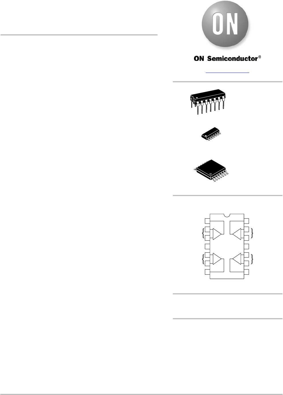
PDIP−14
N SUFFIX
CASE 646
1
14
SOIC−14
D SUFFIX
CASE 751A
1
14
PIN CONNECTIONS
8
Out 4
Inputs 4
V
EE
, GND
Inputs 3
Out 3
9
10
11
12
13
14
2
Out 1
V
CC
Out 2
1
3
4
5
6
7
*
)
Inputs 1
Inputs 2
(Top View)
4
23
1
)
*
*
)
)
*
See general marking information in the device marking
section on page 11 of this data sheet.
DEVICE MARKING INFORMATION
See detailed ordering and shipping information in the package
dimensions section on page 10 of this data sheet.
ORDERING INFORMATION
1
14
TSSOP−14
DTB SUFFIX
CASE 948G
www.onsemi.com

