LM324, LM324A, LM324E, LM224, LM2902, LM2902E, LM2902V, NCV2902
www.onsemi.com
7
V
OR
, OUTPUT VOLTAGE RANGE (V )
pp
V
O
, OUTPUT VOLTAGE (mV)
14
12
10
8.0
6.0
4.0
2.0
0
1.0 10 100 1000
f, FREQUENCY (kHz)
550
500
450
400
350
300
250
200
0
0 1.0 2.0 3.0 4.0 5.0 6.0 7.0 8.0
t, TIME (s)
2.4
2.1
1.8
1.5
1.2
0.9
0.6
0.3
0
0 5.0 10 15 20 25 30 35
V
CC
, POWER SUPPLY VOLTAGE (V) V
CC
, POWER SUPPLY VOLTAGE (V)
90
80
70
0 2.0 4.0 6.0 8.0 10 12 14 16 18 20
I , POWER SUPPLY CURRENT (mA)
CC
I , INPUT BIAS CURRENT (nA)
IB
V
CC
= 30 V
V
EE
= GND
T
A
= 25°C
C
L
= 50 pF
Input
Output
V , INPUT VOLTAGE (V)
I
18
16
14
12
10
8.0
6.0
4.0
2.0
0
20
0 2.0 4.0 6.0 8.0 10 12 14 16 18 20
± V
CC
/V
EE,
POWER SUPPLY VOLTAGES (V)
±
Positive
Negative
T
A
= 25°C
R
L
= R
R
L
= 2.0 k
V
CC
= 15 V
V
EE
= GND
Gain = -100
R
I
= 1.0 k
R
F
= 100 k
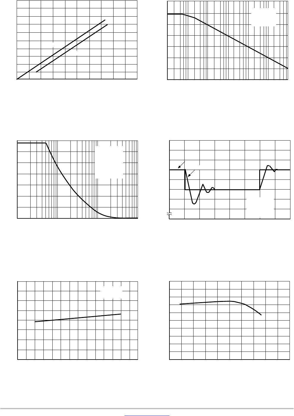
Figure 5. Input Voltage Range
Figure 6. Open Loop Frequency
120
100
80
60
40
20
0
-20
1.0 10 100 1.0 k 10 k 100 k 1.0
M
f, FREQUENCY (Hz)
A , LARGE-SIGNAL
VOL
OPEN LOOP VOLTAGE GAIN (dB)
V
CC
= 15 V
V
EE
= GND
T
A
= 25°C
Figure 7. Large−Signal Frequency Response
Figure 8. Small−Signal Voltage Follower
Pulse Response (Noninverting)
Figure 9. Power Supply Current versus
Power Supply Voltage
Figure 10. Input Bias Current versus
Power Supply Voltage
LM324, LM324A, LM324E, LM224, LM2902, LM2902E, LM2902V, NCV2902
www.onsemi.com
8
2
1
R1
T
BP
R1 + R2
R1
R1 + R2
e
o
e
1
e
2
e
o
= C (1 + a + b) (e
2
- e
1
)
R1
a R1
b R1
R
-
+
+
-
-
+
R
+
-
R1
R2
V
O
V
ref
V
in
V
OH
V
O
V
OL
V
inL
=
R1
(V
OL
- V
ref
) + V
ref
V
inH
=
(V
OH
- V
ref
) + V
ref
H =
R1 + R2
(V
OH
- V
OL
)
R1
-
+
-
+
-
+
R
C
R2
R1
R3
C1
100 k
R
C
R
C1
R2
100 k
V
in
V
ref
V
ref
V
ref
Vref
Bandpass
Output
f
o
=
2 RC
R1 = QR
R2 =
R3 = T
N
R2
C1 = 10C
1
Notch Output
V
ref
=V
CC
Hysteresis
1
C
R
V
inL
V
inH
V
ref
Where:T
BP
=Center Frequency Gain
Where:T
N
=Passband Notch Gain
R = 160 k
C = 0.001 F
R1 = 1.6 M
R2 = 1.6 M
R3 = 1.6 M
For:f
o
=1.0 kHz
For:Q= 10
For:T
BP
= 1
For:T
N
= 1
-
+
MC1403
1/4
LM324
-
+
R1
V
CC
V
CC
V
O
2.5 V
R2
50 k
10 k
V
ref
V
ref
= V
CC
2
5.0 k
R
C
R
C
+
-
V
O
2 RC
1
For: f
o
= 1.0 kHz
R = 16 k
C = 0.01 F
V
O
= 2.5 V 1 +
R1
R2
1
V
CC
f
o
=
1/4
LM324
1/4
LM324
1/4
LM324
1/4
LM324
1
C
R
1/4
LM324
1/4
LM324
1/4
LM324
1/4
LM324
1/4
LM324
Figure 11. Voltage Reference Figure 12. Wien Bridge Oscillator
Figure 13. High Impedance Differential Amplifier Figure 14. Comparator with Hysteresis
Figure 15. Bi−Quad Filter
LM324, LM324A, LM324E, LM224, LM2902, LM2902E, LM2902V, NCV2902
www.onsemi.com
9
2
1
For less than 10% error from operational amplifier,
If source impedance varies, filter may be preceded with
voltage follower buffer to stabilize filter parameters.
where f
o
and BW are expressed in Hz.
Q
o
f
o
BW
< 0.1
Given:f
o
=center frequency
A(f
o
)=gain at center frequency
Choose value f
o
, C
Then:
R3 =
Q
f
o
C
R3
R1 =
2 A(f
o
)
R1 R3
4Q
2
R1 - R3
R2 =
+
-
+
-
V
ref
=V
CC
V
ref
f =
R1 + R
C
4 CR
f
R1
R3 =
R2 R1
R2 + R1
R2
300 k
75 k
R3
R1
100 k
C
Triangle Wave
Output
Square
Wave
Output
V
in
R
f
if
V
ref
1/4
LM324
1/4
LM324
Figure 16. Function Generator Figure 17. Multiple Feedback Bandpass Filter
V
ref
=V
CC
1
2
-
+
V
CC
R3
R1
R2
V
ref
C
C
V
O
CO = 10 C
C
O
1/4
LM324

LM324DTBR2G

Mfr. #:
Manufacturer:
ON Semiconductor
Description:
Operational Amplifiers - Op Amps 3-32V Quad 5mV VIO Commercial Temp
Lifecycle:
New from this manufacturer.
Delivery:
DHL FedEx Ups TNT EMS
Payment:
T/T Paypal Visa MoneyGram Western Union