Data Sheet ADuM4150
Rev. B | Page 3 of 21
SPECIFICATIONS
ELECTRICAL CHARACTERISTICS5 V OPERATION
All typical specifications are at T
A
= 25°C and V
DD1
= V
DD2
= 5 V. Minimum and maximum specifications apply over the entire recommended
operation range: 4.5 V ≤ V
DD1
≤ 5.5 V, 4.5 V ≤ V
DD2
5.5 V, and 40°C T
A
+125°C, unless otherwise noted. Switching specifications
are tested with C
L
= 15 pF and CMOS signal levels, unless otherwise noted.
Table 2. Switching Specifications
Parameter Symbol
Unit Test Conditions/Comments Min Typ Max Min Typ Max
MCLK, MO, SO
SPI Clock Rate SPI
MCLK
10 17 MHz
Data Rate Fast (MO, SO) DR
FAS T
40 40 Mbps Within PWD limit
Propagation Delay t
PHL
, t
PLH
24 12 13 ns 50% input to 50% output
Pulse Width PW 12.5 12.5 ns Within PWD limit
Pulse Width Distortion PWD 2 2 ns |t
PLH
− t
PHL
|
Codirectional Channel Matching
1
t
PSKCD
2 2 ns
Jitter, High Speed J
HS
1 1 ns
MSS
Data Rate Fast DR
FAS T
40 40 Mbps Within PWD limit
Propagation Delay t
PHL
, t
PLH
21 24 21 24 ns 50% input to 50% output
Pulse Width PW 12.5 12.5 ns Within PWD limit
Pulse Width Distortion PWD 2 2 ns |t
PLH
− t
PHL
|
Setup Time
2
MSS
SETUP
1.5 10 ns
Jitter, High Speed J
HS
1 1 ns
DCLK
3
Data Rate
40
40
MHz
Propagation Delay t
PHL
, t
PLH
50 35 ns t
PMCLK
+ t
PSO
+ 3 ns
Pulse Width Distortion PWD 3 3 ns |t
PLH
− t
PHL
|
Pulse Width PW 12 12 ns Within PWD limit
Clock Delay Error DCLK
ERR
0 4.5 12 1 5.5 12 ns t
PDCLK
(t
PMCLK
+ t
PSO
)
Jitter J
DCLK
1 1 ns
V
IA
, V
IB
Data Rate Slow DR
SLOW
250 250 kbps Within PWD limit
Propagation Delay t
PHL
, t
PLH
0.1 2.6 0.1 2.6 µs 50% input to 50% output
Pulse Width PW 4 4 µs Within PWD limit
Jitter, Low Speed J
LS
2.5 2.5 µs
V
Ix
4
Minimum Input Skew
5
t
VIx SKEW
10 10 ns
1
Codirectional channel matching is the absolute value of the difference in propagation delays between any two channels with inputs on the same side of the isolation barrier.
2
The
MSS
signal is glitch filtered in both speed grades, whereas the other fast signals are not glitch filtered in the B grade. To guarantee that
MSS
reaches the output
ahead of another fast signal, set up
MSS
prior to the competing signal by different times depending on speed grade.
3
t
PMCLK
is the propagation delay of the MCLK signal from Side 1 to Side 2. t
PSO
is the propagation delay of the SO signal from Side 2 to Side 1. t
PDCLK
is the difference
between the DCLK signal and the round trip propagation delay.
4
V
Ix
= V
IA
or V
IB
.
5
An internal asynchronous clock, not available to users, samples the low speed signals. If edge sequence in codirectional channels is critical to the end application, the
leading pulse must be at least 1 t
VIx SKEW
time ahead of a later pulse to guarantee the correct order or simultaneous arrival at the output.
ADuM4150 Data Sheet
Rev. B | Page 4 of 21
Table 3. For All Grades
1, 2, 3
Parameter Symbol Min Typ Max Unit Test Conditions/Comments
SUPPLY CURRENT
1 MHz, A Grade and B Grade I
DD1
5 8.5 mA C
L
= 0 pF, DR
FAS T
= 1 MHz,
DR
SLOW
= 0 MHz
I
DD2
6.5 11 mA C
L
= 0 pF, DR
FAS T
= 1 MHz,
DR
SLOW
= 0 MHz
17 MHz, B Grade I
DD1
15 23 mA C
L
= 0 pF, DR
FAS T
= 17 MHz,
DR
SLOW
= 0 MHz
I
DD2
13.5 21 mA C
L
= 0 pF, DR
FAS T
= 17 MHz,
DR
SLOW
= 0 MHz
DC SPECIFICATIONS
MCLK,
MSS
, MO, SO, V
IA
, V
IB
Input Threshold
Logic High V
IH
0.7 × V
DDx
V
Logic Low V
IL
0.3 × V
DDx
V
Input Hysteresis V
IHYST
500 mV
Input Current per Channel I
I
−1 +0.01 +1 µA 0 V ≤ V
INPUT
≤ V
DDx
SCLK,
SSS
, MI, SI, V
OA
, V
OB
, DCLK
Output Voltages
Logic High V
OH
V
DDx
− 0.1 5.0 V I
OUTPUT
= −20 µA, V
INPUT
= V
IH
V
DDx
− 0.4 4.8 V I
OUTPUT
= −4 mA, V
INPUT
= V
IH
Logic Low V
OL
0.0 0.1 V I
OUTPUT
= 20 µA, V
INPUT
= V
IL
0.2 0.4 V I
OUTPUT
= 4 mA, V
INPUT
= V
IL
V
DD1
, V
DD2
Undervoltage Lockout UVLO 2.6 V
Supply Current per High Speed Channel
Dynamic Input I
DDI(D)
0.080 mA/Mbps
Dynamic Output I
DDO(D)
0.046 mA/Mbps
Supply Current for All Low Speed Channels
Quiescent Side 1 Current I
DD1(Q)
4.4 mA
Quiescent Side 2 Current I
DD2(Q)
6.1 mA
AC SPECIFICATIONS
Output Rise/Fall Time t
R
/t
F
2.5 ns 10% to 90%
Common-Mode Transient Immunity
4
|CM|
25
35
kV/µs
V
INPUT
= V
DDx
, V
CM
= 1000 V,
transient magnitude = 800 V
1
V
DDx
= V
DD1
or V
DD2
.
2
V
INPUT
is the input voltage of any of the MCLK,
MSS
, MO, SO, V
IA
, or V
IB
pins.
3
I
OUTPUT
is the output current of any of the SCLK, DCLK,
SSS
, MI, SI, V
OA
, or V
OB
pins.
4
|CM| is the maximum common-mode voltage slew rate that can be sustained while maintaining output voltages within the V
OH
and V
OL
limits. The common-mode
voltage slew rates apply to both rising and falling common-mode voltage edges.
Data Sheet ADuM4150
Rev. B | Page 5 of 21
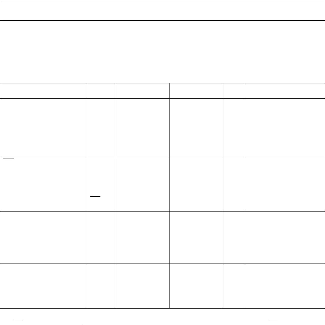
ELECTRICAL CHARACTERISTICS—3.3 V OPERATION
All typical specifications are at T
A
= 25°C and V
DD1
= V
DD2
= 3.3 V. Minimum and maximum specifications apply over the entire recommended
operation range: 3.0 V ≤ V
DD1
≤ 3.6 V, 3.0 V ≤ V
DD2
≤ 3.6 V, and −40°C T
A
+125°C, unless otherwise noted. Switching specifications
are tested with C
L
= 15 pF and CMOS signal levels, unless otherwise noted.
Table 4. Switching Specifications
Parameter Symbol
A Grade B Grade
Unit Test Conditions/Comments Min Typ Max Min Typ Max
MCLK, MO, SO
SPI Clock Rate SPI
MCLK
8.3 12.5 MHz
Data Rate Fast (MO, SO) DR
FAS T
40 40 Mbps Within PWD limit
Propagation Delay t
PHL
, t
PLH
30 20 ns 50% input to 50% output
Pulse Width PW 12.5 12.5 ns Within PWD limit
Pulse Width Distortion PWD 3 3 ns |t
PLH
− t
PHL
|
Codirectional Channel Matching
1
t
PSKCD
3 3 ns
Jitter, High Speed
J
HS
1
1
ns
MSS
Data Rate Fast DR
FAS T
40 40 Mbps Within PWD limit
Propagation Delay t
PHL
, t
PLH
30 30 ns 50% input to 50% output
Pulse Width PW 12.5 12.5 ns Within PWD limit
Pulse Width Distortion PWD 3 3 ns |t
PLH
− t
PHL
|
Setup Time
2
MSS
SETUP
1.5 10 ns
Jitter, High Speed J
HS
1 1 ns
DCLK
3
Data Rate 40 40 MHz
Propagation Delay t
PHL
, t
PLH
60 40 ns t
PMCLK
+ t
PSO
+ 3 ns
Pulse Width Distortion PWD 3 3 ns |t
PLH
− t
PHL
|
Pulse Width PW 12 12 ns Within PWD limit
Clock Delay Error DCLK
ERR
−4 +2.4 +9 −3 +2.5 +8 ns t
PDCLK
(t
PMCLK
+ t
PSO
)
Jitter J
DCLK
1 1 ns
V
IA
, V
IB
Data Rate Slow DR
SLOW
250 250 kbps Within PWD limit
Propagation Delay t
PHL
, t
PLH
0.1 2.6 0.1 2.6 µs 50% input to 50% output
Pulse Width PW 4 4 µs Within PWD limit
Jitter, Low Speed J
LS
2.5 2.5 µs
V
Ix
4
Minimum Input Skew
5
t
VIx SKEW
10 10 ns
1
Codirectional channel matching is the absolute value of the difference in propagation delays between any two channels with inputs on the same side of the isolation barrier.
2
The
MSS
signal is glitch filtered in both speed grades, whereas the other fast signals are not glitch filtered in the B grade. To guarantee that
MSS
reaches the output
ahead of another fast signal, set up
MSS
prior to the competing signal by different times depending on speed grade.
3
t
PMCLK
is the propagation delay of the MCLK signal from Side 1 to Side 2. t
PSO
is the propagation delay of the SO signal from Side 2 to Side 1. t
PDCLK
is the difference
between the DCLK signal and the round trip propagation delay.
4
V
Ix
= V
IA
or V
IB
.
5
An internal asynchronous clock, not available to users, samples the low speed signals. If edge sequence in codirectional channels is critical to the end application, the
leading pulse must be at least 1 t
VIx SKEW
time ahead of a later pulse to guarantee the correct order or simultaneous arrival at the output.

ADUM4150ARIZ

Mfr. #:
Manufacturer:
Analog Devices Inc.
Description:
Digital Isolators 6 Ch 40 MHz Iso lator for Interface
Lifecycle:
New from this manufacturer.
Delivery:
DHL FedEx Ups TNT EMS
Payment:
T/T Paypal Visa MoneyGram Western Union

Products related to this Datasheet